1.1 Definition of white light CSP
LED white light CSP has gradually moved from concept to mature product through the hard work of R&D in the industry for several years. In particular, CSP based on flip chip development has been applied to high-end applications such as backlight, flashlight, and commercial lighting due to its excellent light extraction efficiency, good heat dissipation structure, and compact external dimensions.
The CSP structures developed by various manufacturers are different, and are roughly divided into the following categories, as shown in Figure 1.

Figure 1 LED CSP structure diagram
Structure A: The fluorescent film covers the flip-chip LED chip to form a 5-sided light-emitting CSP structure.
Structure B: Changed from structure A, using white reflective silica gel as a vertical wall surface to form a single-sided light-emitting structure. This structure is also the current CSP style in the field of flash, backlight and other applications.
Structure C: This structure is applied to a potted LED package with a white reflector, using a non-tacky fluorescent film, and is also a single-sided light-emitting structure. Similar structures are already mature on the package of the packaged chip.
Structure D: A 50-70 micron ultra-thin fluorescent layer is formed on the chip by spraying a fluorescent glue, and then sealed with a transparent silica gel in a reflective cup.
The core feature of each structure is that the package resin has a five-sided cladding with a thickness of about 50-150 um for the flip chip, and only one side of the exposed electrode is formed to form a single-sided or five-sided light-emitting package structure.
From the packaging process point of view, CSP can be made by spraying, molding, laminating cured non-tacky fluorescent film, laminating semi-cured fluorescent film, etc., so the major manufacturers hold their own academic definitions or commercial naming of CSP. Viewpoints such as WIPCO, PFOC, NCSP.
From the perspective of self-developed packaging materials and packaging technology, Degao Chemicals has proposed a structure for the five-sided light-emitting structure A, named PFCC, which is a phosphor film coated chip, which is made by flip-chip mounting with a fluorescent film. CSP.
1.2 Process development characteristics of white light PFCC type CSP
The PFCC adopts the semi-cured premixed fluorescent powder silica gel membrane TAPIT developed by Dega Chemicals Co., Ltd., and the packaged LED flip-chip vacuum thermocompression or roll bonding to complete the encapsulation. The packaged silica gel is cured at a high temperature and mechanically cut to obtain an independent CSP chip. The package process diagram is shown in Figure 2.

Figure 2 Schematic diagram of the production process of five-sided PFCC
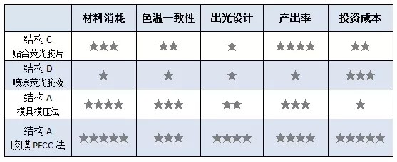
Combined with the package structure and manufacturing process of the above various CSPs, we can compare the structure and design advantages of various CSPs.

Table 1 Performance comparison between CSP structure and manufacturing process
1. PFCC packaging material consumption advantage
The important support for CSP to significantly reduce packaging costs comes from less packaging material consumption. Using the PFCC process, the chip package adhesive thickness can be designed in the range of 70-150um, combined with the process capability of the cutting process, the chip can be arrayed at 300-400um pitch.
Taking a 40×40 mil chip as an example, a crystallographic region (about 45 mm×90 mm crystallization region) of about 2050 chips is formed according to a crystal spacing of 400 um, and a PACKAGE thickness of about 300 um is controlled, and a fluorescent film is added (according to 30% by weight) Phosphor) is used in an amount of only 4 g.
Spraying or extrusion coating of fluorescent glue method, although the unit cost of the material is not high, but the mixing time of the two-component silica gel and the phosphor, the operation time is difficult to control, the phosphor sedimentation leads to bad waste and other factors, so that the overall cost needs to be comprehensively evaluated.
High-voltage Electric Pole is a high-rise structure that supports high-voltage transmission lines. They are a vital part of the power grid, helping to move electricity from power plants to homes, businesses and other buildings. High-voltage power poles are marked with warning signs alerting people to the dangers of electrocution and are often located in areas where access is restricted to prevent accidents.
High Voltage Electric Pole,Power Line Pole,Steel Transmission Poles,Galvanized Electric Pole
JIANGSU HONGGUANG STEEL POLE CO., LTD. , https://www.hgsteelpoles.com