Abstract: This application note proposes a design idea for an ultra-low jitter clock synthesizer. Its goal is to generate a 2GHz clock with jitter between edges <100fs. Analysis and simulation results show that to achieve this jitter index, the design difficulty is much higher than expected. Discussions on component variables and trade-offs provide clues for further research.
Overview This article provides a reference design for a low-jitter clock source for high-speed data converters. The goal is to achieve edge-to-edge jitter <100fs at clock frequencies up to 2GHz. For the 1GHz analog output frequency, the resulting jitter signal-to-noise ratio SNR is: -20 × log (2 × π × f × tj) = -64dB.
Design requirements The maximum frequency of the clock design is 2GHz. However, some VCOs (voltage controlled oscillators) and prescalers can be extended to higher frequencies, and the range that different devices can extend is not the same. The reference design, simulation tests and results presented here are only for the 2GHz output frequency.
Some high-speed converters use both edges of the clock signal as internal timing. This requires a strict 50% duty cycle. In addition, the target output drive capability is 10dBm / 50Ω, which is the 2VP-P differential output.
Synthesizer design basics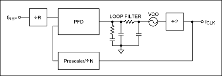
Figure 1. Traditional phase-locked loop
The simplest design is a traditional phase-locked loop circuit, as shown in Figure 1. As mentioned above, a strict 50% duty cycle is required. Therefore, the VCO works at twice the frequency of the target clock (4GHz), and then obtains the target frequency and duty cycle by dividing by 2. Since the frequency divider introduces jitter, it is placed in a phase-locked loop loop to eliminate noise.
The loop filter provides low-pass filtering of reference noise and high-pass filtering of VCO noise. At the same time, it also determines the loop establishment time. Since this is a fixed frequency application, there is no problem with the loop settling time; the filter bandwidth can only be optimized for noise. Narrowband filters are easier to handle reference noise, but increase the noise burden of the VCO, and the effect of wideband filters is the opposite.
Although we need to balance between the VCO and the reference clock, research on both shows that it is possible to obtain the best performance of both. The phase noise index of 100fs jitter determines how low the noise will be.
Phase noise is an index relative to the carrier frequency and inversely proportional to the frequency deviation (dBc / Hz). The set of all phase noise is the phase noise power, which is used to compare with the fundamental frequency power. The phase noise is divided by the fundamental frequency power to obtain jitter.
For example, suppose a 2GHz VCO has an SSB (single sideband) phase noise of -110dBc / Hz from 10kHz to 100kHz, and its bandwidth is 90kHz, resulting in 49.5dB. Therefore, the total noise is -60.5dBc. The SSB noise power is:

Therefore, the effective value of the noise voltage is:

The factor 2 in the root sign represents the inclusion of two single sidebands¹.
Its jitter is:

Equation 3 only yields jitter at a frequency offset of 10kHz to 100kHz. In order to determine the overall jitter, the remaining frequency offset must also be considered.
Another method is that we reverse phase noise from jitter. So, for 100fs jitter at 2GHz:

The SSB noise power is:

The result of Equation 5 is equivalent to the total noise power (SSB) of -61dBc. If it is assumed that the phase noise is evenly distributed from 1 Hz to 10 MHz, then, converted to dBc / Hz, the following phase noise template is obtained (Figure 2).
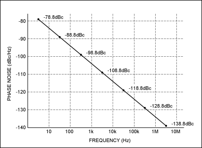
Figure 2. Phase noise template
There is no doubt that jitter <100fs at 2GHz is a very good phase noise value, especially in the range of 10kHz to 100kHz. It can be seen from the figure that the phase noise at 10kHz is approximately -114dBc / Hz. But very few separate VCOs can achieve this level. Of course, it is difficult to achieve this goal with integrated VCOs. UMC (Universal Microwave CorporaTIon) VCO can achieve this low noise level. The bandwidth of UMX series products is 500MHz to 5GHz, and its 10kHz phase noise can reach below -112dBc / Hz. Even the worst VCO in the UMX series meets our requirements.
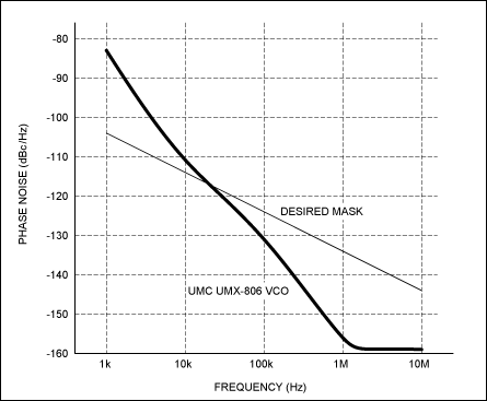
Figure 3. UMX-806-D16 corresponds to the phase noise of the phase noise template
Figure 3 shows the worst-case phase noise of the 4GHz VCO (UMX-806-D16) and our target phase noise template. The phase noise of the VCO below 20kHz is very high, but by designing the bandwidth of the phase-locked loop filter, low-frequency partial VCO noise can be suppressed. Assuming that there are no other factors, a good phase noise index above 10kHz can be obtained. Please note that these phase noise requirements come from a 2GHz oscillator. However, Figure 3 shows the curve of the 4GHz oscillator, which requires an additional divide by 2 to ensure a 50% duty cycle. Assuming that the frequency division by 2 itself does not affect the total phase noise, the phase noise of the VCO will be reduced by 6dB, and the entire curve will shift down by 6dB in parallel.
Note that the reference clock also generates noise, but most of it is distributed below the loop filter bandwidth. Figure 4 shows the Bert diagram of Crystek® 80MHz crystal voltage controlled oscillator and the target phase noise template. Note that the frequency gain of the phase-locked loop will amplify the phase noise of the reference clock in equal times. Therefore, for 80MHz crystal and 2GHz output, the gain is 25. As a result, the Crystek curve will shift up 28dB. This translation means that the phase noise of the reference clock is very high at 1kHz³. However, the phase noise template assumes that the total noise power is evenly distributed within the frequency offset. Of course, this is not necessarily the case, so constant phase noise outside 1kHz plus noise within 1kHz can still meet our jitter specifications.
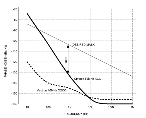
Figure 4. Phase noise of the reference clock
The phase noise analysis in Figure 4 also includes a Vectron constant temperature controlled oscillator (OCXO), which has extremely low phase noise. Note that OCXO easily consumes more power (up to the watt level).
Synthesizer Schematic Figure 5 is the complete circuit schematic of the reference clock and VCO discussed earlier. The PLL uses Fujitsu® MB15E06SR, which integrates a 4mA charge pump and a prescaler up to 3GHz. Because the PLL needs to be programmed, we have adopted a very simple PIC microprocessor (PIC18F2455) with a built-in USB interface that can automatically perform programming tasks. This design requires software to program the user interface, as well as PIC.
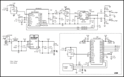
Clear picture (PDF, 93.8KB)
Figure 5. Schematic diagram of the clock synthesizer
The frequency divider uses HitTIte® HMC361, which can work up to 10GHz, and its phase noise has little effect on performance. However, the output swing of the crossover is only 0.8VP-P, or 2dBm at 50Ω. The design goal is 10dBm output (2VP-P), so the output of HitTIte cannot meet the requirements, and the voltage needs to be increased. On Semiconductor® or Zarlink® have similar products, but their output swings are basically the same as HitTIte, or even worse. Moreover, their noise specifications are not clearly marked.
A simple transformer can be used to increase the swing of a low-speed clock, but transformers above 2GHz that can achieve 4: 1 amplification are not common. In addition, this approach increases the difficulty of impedance design. Another method is to use active amplifiers, which can obtain many differential amplifiers with bandwidths> 10GHz, but the noise specifications of the device need to be further determined to meet the design requirements. Another question is whether the amplifier can be placed in the PLL. Fujitsu data sheets recommend a maximum prescaler input of 2dBm (1VP-P).
Simulation results ADIsimPLL (written by Applied Radio Labs for Analog Devices) can be used to analyze the circuit, which includes multiple UMC VCO models. Figure 6 shows the PLL phase noise Bert diagram composed of UMC 4GHz VCO without frequency divider and Crystek oscillator. Below 2kHz, the noise of the reference clock dominates; above 2kHz, the phase detector phase noise dominates; above 70kHz, the VCO noise dominates.
Fig. 6 includes the target noise template (thick black line) of Fig. 2. Obviously, the total noise exceeds the template below 50kHz, which will produce 200fs of jitter. There is a problem in actual simulation, that is, how to solve the phase noise of the phase detector. It should be equal to the noise floor of a particular device (-219dBc / Hz) multiplied by the VCO / PFD frequency, which is 4000MHz / 25MHz, or 44dB, shifted 118dB. Further verification is required, but even if the PFD (Phase Detector) noise is removed, the result is still unacceptable (167fs).
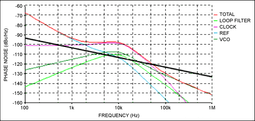
Figure 6. Simulation results using VCO: phase noise at 4GHz
In addition to PFD noise, the filter setting is close to the VCO noise peak at 10kHz. The main remaining problem is the reference clock noise. Unfortunately, the performance better than the template above 40kHz is not enough to eliminate this noise. Therefore, other types of oscillators need to be used to meet the phase noise requirements, such as: OCXO.
The printed circuit board (PCB) of this design can be adapted to three or four different XO pinouts. Figure 7 shows the simulation results using Vectron OCXO. Even considering the phase detector noise, the final jitter is 86.5fs. This jitter leaves a certain margin for the crossover noise that is not considered (the noise should have no significant negative effects) and the amplifier that may be needed.
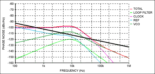
Figure 7. Simulation results using Vectron OXCO: phase noise at 4GHz
Conclusion The jitter target of 100fs at 2GHz is more difficult to achieve than we expected. Experimental data shows that using some standard PLL circuits can achieve this goal. The key lies in the choice of VCO and reference clock. Experiments show that UMX's VCO has first-class phase noise performance. The remaining two problems are: (1) select a reference clock with sufficiently low noise; (2) select a suitable amplifier. Fortunately, we have many devices to choose from, and the same circuit layout can be applied to different types of pin arrangements. The choice of amplifier is more difficult, and further analysis is needed to determine whether it can be placed in the loop, and the impact of its noise needs to be considered.
¹Considering two single sidebands, the factor 2 is included both inside and outside the radical. The total noise power is twice the SSB noise power, so the total noise voltage should be equal to the SSB noise voltage.
² refers to a single component, not a module.
³High phase noise around 1MHz, but the loop filter helps to attenuate this noise.
Overview This article provides a reference design for a low-jitter clock source for high-speed data converters. The goal is to achieve edge-to-edge jitter <100fs at clock frequencies up to 2GHz. For the 1GHz analog output frequency, the resulting jitter signal-to-noise ratio SNR is: -20 × log (2 × π × f × tj) = -64dB.
Design requirements The maximum frequency of the clock design is 2GHz. However, some VCOs (voltage controlled oscillators) and prescalers can be extended to higher frequencies, and the range that different devices can extend is not the same. The reference design, simulation tests and results presented here are only for the 2GHz output frequency.
Some high-speed converters use both edges of the clock signal as internal timing. This requires a strict 50% duty cycle. In addition, the target output drive capability is 10dBm / 50Ω, which is the 2VP-P differential output.
Synthesizer design basics

Figure 1. Traditional phase-locked loop
The simplest design is a traditional phase-locked loop circuit, as shown in Figure 1. As mentioned above, a strict 50% duty cycle is required. Therefore, the VCO works at twice the frequency of the target clock (4GHz), and then obtains the target frequency and duty cycle by dividing by 2. Since the frequency divider introduces jitter, it is placed in a phase-locked loop loop to eliminate noise.
The loop filter provides low-pass filtering of reference noise and high-pass filtering of VCO noise. At the same time, it also determines the loop establishment time. Since this is a fixed frequency application, there is no problem with the loop settling time; the filter bandwidth can only be optimized for noise. Narrowband filters are easier to handle reference noise, but increase the noise burden of the VCO, and the effect of wideband filters is the opposite.
Although we need to balance between the VCO and the reference clock, research on both shows that it is possible to obtain the best performance of both. The phase noise index of 100fs jitter determines how low the noise will be.
Phase noise is an index relative to the carrier frequency and inversely proportional to the frequency deviation (dBc / Hz). The set of all phase noise is the phase noise power, which is used to compare with the fundamental frequency power. The phase noise is divided by the fundamental frequency power to obtain jitter.
For example, suppose a 2GHz VCO has an SSB (single sideband) phase noise of -110dBc / Hz from 10kHz to 100kHz, and its bandwidth is 90kHz, resulting in 49.5dB. Therefore, the total noise is -60.5dBc. The SSB noise power is:

Therefore, the effective value of the noise voltage is:

The factor 2 in the root sign represents the inclusion of two single sidebands¹.
Its jitter is:

Equation 3 only yields jitter at a frequency offset of 10kHz to 100kHz. In order to determine the overall jitter, the remaining frequency offset must also be considered.
Another method is that we reverse phase noise from jitter. So, for 100fs jitter at 2GHz:

The SSB noise power is:

The result of Equation 5 is equivalent to the total noise power (SSB) of -61dBc. If it is assumed that the phase noise is evenly distributed from 1 Hz to 10 MHz, then, converted to dBc / Hz, the following phase noise template is obtained (Figure 2).

Figure 2. Phase noise template
There is no doubt that jitter <100fs at 2GHz is a very good phase noise value, especially in the range of 10kHz to 100kHz. It can be seen from the figure that the phase noise at 10kHz is approximately -114dBc / Hz. But very few separate VCOs can achieve this level. Of course, it is difficult to achieve this goal with integrated VCOs. UMC (Universal Microwave CorporaTIon) VCO can achieve this low noise level. The bandwidth of UMX series products is 500MHz to 5GHz, and its 10kHz phase noise can reach below -112dBc / Hz. Even the worst VCO in the UMX series meets our requirements.

Figure 3. UMX-806-D16 corresponds to the phase noise of the phase noise template
Figure 3 shows the worst-case phase noise of the 4GHz VCO (UMX-806-D16) and our target phase noise template. The phase noise of the VCO below 20kHz is very high, but by designing the bandwidth of the phase-locked loop filter, low-frequency partial VCO noise can be suppressed. Assuming that there are no other factors, a good phase noise index above 10kHz can be obtained. Please note that these phase noise requirements come from a 2GHz oscillator. However, Figure 3 shows the curve of the 4GHz oscillator, which requires an additional divide by 2 to ensure a 50% duty cycle. Assuming that the frequency division by 2 itself does not affect the total phase noise, the phase noise of the VCO will be reduced by 6dB, and the entire curve will shift down by 6dB in parallel.
Note that the reference clock also generates noise, but most of it is distributed below the loop filter bandwidth. Figure 4 shows the Bert diagram of Crystek® 80MHz crystal voltage controlled oscillator and the target phase noise template. Note that the frequency gain of the phase-locked loop will amplify the phase noise of the reference clock in equal times. Therefore, for 80MHz crystal and 2GHz output, the gain is 25. As a result, the Crystek curve will shift up 28dB. This translation means that the phase noise of the reference clock is very high at 1kHz³. However, the phase noise template assumes that the total noise power is evenly distributed within the frequency offset. Of course, this is not necessarily the case, so constant phase noise outside 1kHz plus noise within 1kHz can still meet our jitter specifications.

Figure 4. Phase noise of the reference clock
The phase noise analysis in Figure 4 also includes a Vectron constant temperature controlled oscillator (OCXO), which has extremely low phase noise. Note that OCXO easily consumes more power (up to the watt level).
Synthesizer Schematic Figure 5 is the complete circuit schematic of the reference clock and VCO discussed earlier. The PLL uses Fujitsu® MB15E06SR, which integrates a 4mA charge pump and a prescaler up to 3GHz. Because the PLL needs to be programmed, we have adopted a very simple PIC microprocessor (PIC18F2455) with a built-in USB interface that can automatically perform programming tasks. This design requires software to program the user interface, as well as PIC.

Clear picture (PDF, 93.8KB)
Figure 5. Schematic diagram of the clock synthesizer
The frequency divider uses HitTIte® HMC361, which can work up to 10GHz, and its phase noise has little effect on performance. However, the output swing of the crossover is only 0.8VP-P, or 2dBm at 50Ω. The design goal is 10dBm output (2VP-P), so the output of HitTIte cannot meet the requirements, and the voltage needs to be increased. On Semiconductor® or Zarlink® have similar products, but their output swings are basically the same as HitTIte, or even worse. Moreover, their noise specifications are not clearly marked.
A simple transformer can be used to increase the swing of a low-speed clock, but transformers above 2GHz that can achieve 4: 1 amplification are not common. In addition, this approach increases the difficulty of impedance design. Another method is to use active amplifiers, which can obtain many differential amplifiers with bandwidths> 10GHz, but the noise specifications of the device need to be further determined to meet the design requirements. Another question is whether the amplifier can be placed in the PLL. Fujitsu data sheets recommend a maximum prescaler input of 2dBm (1VP-P).
Simulation results ADIsimPLL (written by Applied Radio Labs for Analog Devices) can be used to analyze the circuit, which includes multiple UMC VCO models. Figure 6 shows the PLL phase noise Bert diagram composed of UMC 4GHz VCO without frequency divider and Crystek oscillator. Below 2kHz, the noise of the reference clock dominates; above 2kHz, the phase detector phase noise dominates; above 70kHz, the VCO noise dominates.
Fig. 6 includes the target noise template (thick black line) of Fig. 2. Obviously, the total noise exceeds the template below 50kHz, which will produce 200fs of jitter. There is a problem in actual simulation, that is, how to solve the phase noise of the phase detector. It should be equal to the noise floor of a particular device (-219dBc / Hz) multiplied by the VCO / PFD frequency, which is 4000MHz / 25MHz, or 44dB, shifted 118dB. Further verification is required, but even if the PFD (Phase Detector) noise is removed, the result is still unacceptable (167fs).

Figure 6. Simulation results using VCO: phase noise at 4GHz
In addition to PFD noise, the filter setting is close to the VCO noise peak at 10kHz. The main remaining problem is the reference clock noise. Unfortunately, the performance better than the template above 40kHz is not enough to eliminate this noise. Therefore, other types of oscillators need to be used to meet the phase noise requirements, such as: OCXO.
The printed circuit board (PCB) of this design can be adapted to three or four different XO pinouts. Figure 7 shows the simulation results using Vectron OCXO. Even considering the phase detector noise, the final jitter is 86.5fs. This jitter leaves a certain margin for the crossover noise that is not considered (the noise should have no significant negative effects) and the amplifier that may be needed.

Figure 7. Simulation results using Vectron OXCO: phase noise at 4GHz
Conclusion The jitter target of 100fs at 2GHz is more difficult to achieve than we expected. Experimental data shows that using some standard PLL circuits can achieve this goal. The key lies in the choice of VCO and reference clock. Experiments show that UMX's VCO has first-class phase noise performance. The remaining two problems are: (1) select a reference clock with sufficiently low noise; (2) select a suitable amplifier. Fortunately, we have many devices to choose from, and the same circuit layout can be applied to different types of pin arrangements. The choice of amplifier is more difficult, and further analysis is needed to determine whether it can be placed in the loop, and the impact of its noise needs to be considered.
¹Considering two single sidebands, the factor 2 is included both inside and outside the radical. The total noise power is twice the SSB noise power, so the total noise voltage should be equal to the SSB noise voltage.
² refers to a single component, not a module.
³High phase noise around 1MHz, but the loop filter helps to attenuate this noise.
Sfp Fiber Adapter,St Fiber Coupler,St Fiber To Ethernet Converter,Sfp To Sc Adapter
Ningbo Fengwei Communication Technology Co., Ltd , https://www.fengweifiberoptic.com