MOSFET body diode characteristics
The origin of parasitic diodes
It is caused by the production process. The drain of the high-power MOS transistor is taken out from the bottom of the silicon wafer. This parasitic diode will be present. A low-power MOS transistor, such as an MOS transistor in an integrated chip, has a planar structure, and the drain lead-out direction is from the top of the silicon chip, that is, the same direction as the source and the like, without this diode. The analog circuit book speaks of the structure of a low-power MOS tube, so there is no such diode. However, there is a parasitic diode between the D-pole and the substrate. If it is a single transistor, the substrate is naturally connected to the S-pole, so naturally there is a diode between the DSs. If in the IC, the N-MOS substrate is connected to the lowest voltage, the P-MOS substrate is connected to the highest voltage, not necessarily connected to the S pole, so there is not necessarily a parasitic diode between the DS.
Parasitic diode function:
When a large instantaneous reverse current occurs in the circuit, it can be derived from this diode so as not to break through the MOS transistor. (Play the role of protection MOS tube)
The structure of the trench Trench type N-channel enhancement type power MOSFET is as shown in the figure below. The P base region is diffused on the N-epi epitaxial layer, and then the trench is formed by an etching technique to a depth deeper than that of the P base region. The upper thermal oxidation generates a gate oxide layer, and the polysilicon is used to fill the trench. The N+ source region is formed by a self-aligned process, and the N+substrate on the back side is a drain region. After a certain positive voltage is applied to the gate, the sidewall of the trench is P The base area is inverted and vertical channels are formed.
As can be seen from the structure in the figure below, the P base and N-epi form a PN junction, which is the parasitic body diode of the MOSFET.
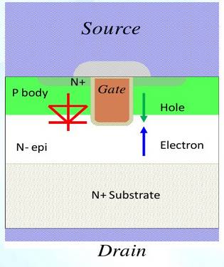
MOSFET profile structure
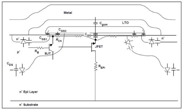
Body diode main parameters

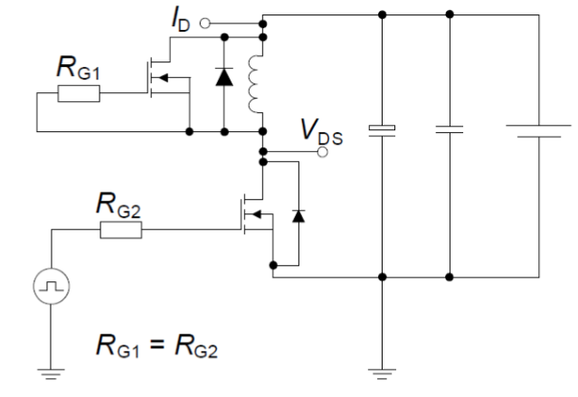
Diode characteristics test circuit
Diode recovery curve
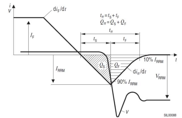
MOSFET body diode reverse recovery process waveform
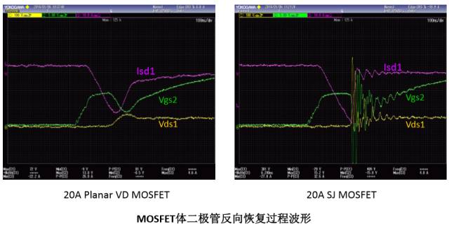
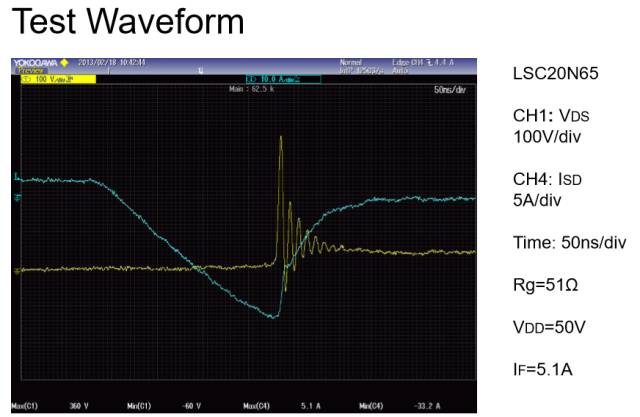
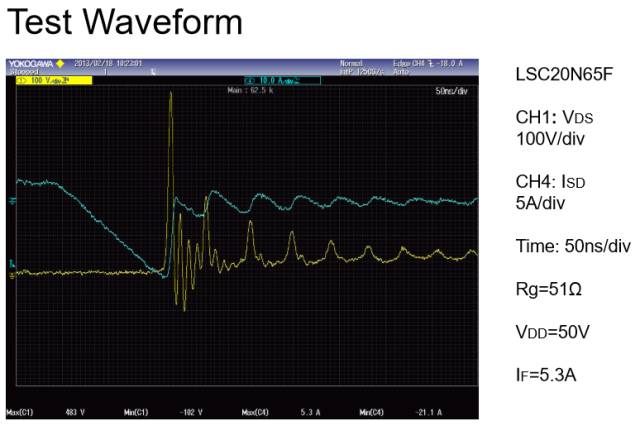
MOSFET Body Diode Applications

Full-bridge inverter circuit
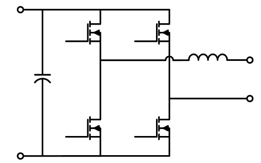
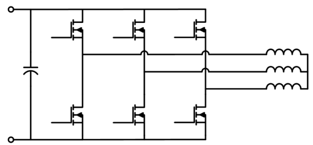
Three-phase bridge circuit
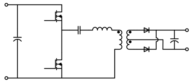
LLC Half-Bridge Resonant Circuit ZVS
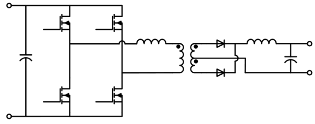
Phase-shifted full-bridge PSFB ZVS
HID Lighting (ZVS)

MOSFET body diode application analysis 
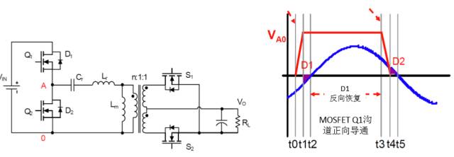
MOSFET body diode reverse recovery
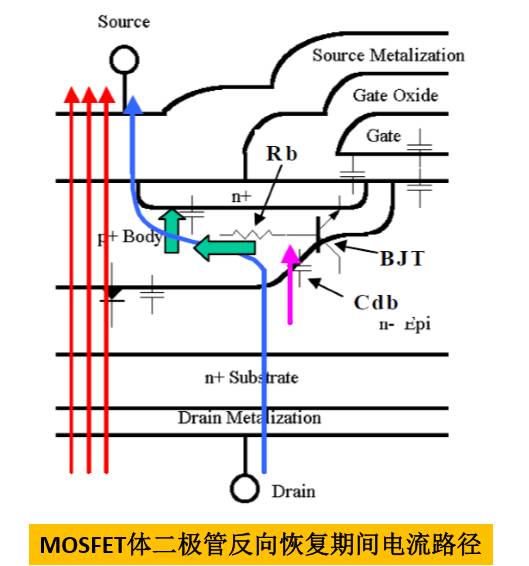
LLC Half-Bridge Resonant Converter
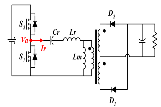
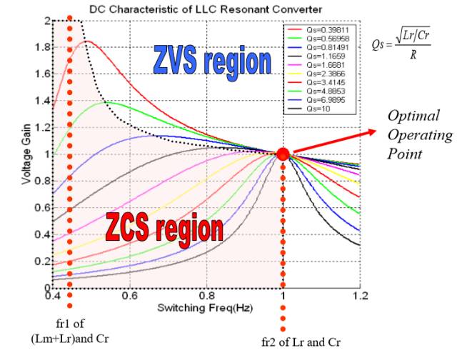
LLC voltage gain
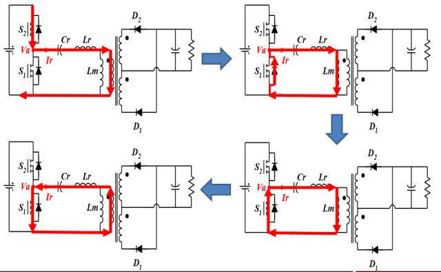
LLC Converter Mode Switching in ZVS State
LLC Converter Operation Waveform (ZVS Mode)
LLC Converter Operation Waveform (ZVS Mode, Light Load)

LLC Converter Mode Switching in ZCS State
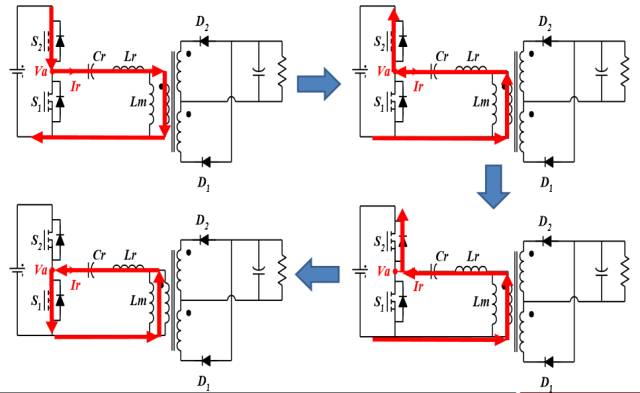
LLC Converter Operation Waveform
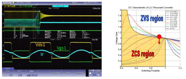
LLC Converter Output Short Status 1 Waveform
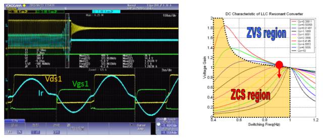
LLC Converter Output Short State 2 Waveform
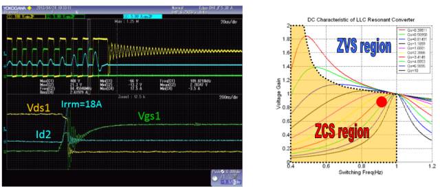
LLC Startup Process - Diode Reverse Recovery

LLC Startup Process - Diode Reverse Recovery
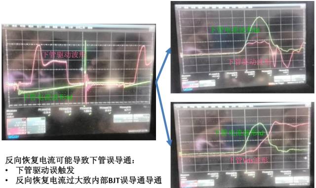
HID lighting power supply (with load switching to open circuit)

HID lighting power startup process
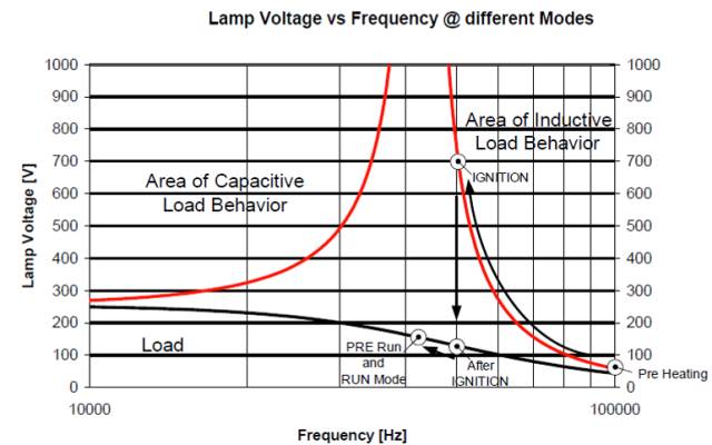
HID Lighting Power Supply (Working Waveform Below Resonance Frequency)
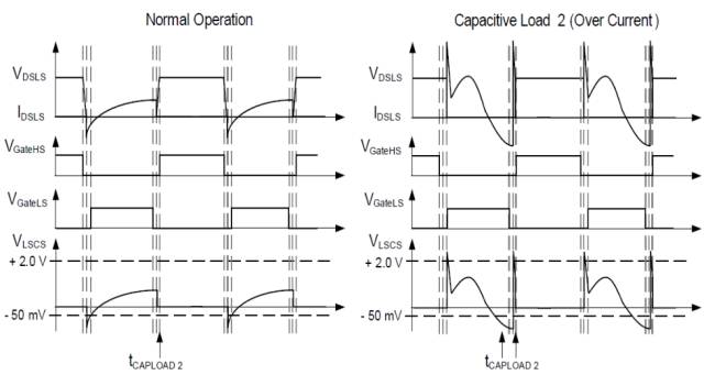
HID lighting power measurement waveform

Zysen provide RF High Power Pin Switch, 2 to 16 way, controlled by TTL, power up to 100W, Customized frequency and optimized specifications available. Contact us with your requirement.
Rf Coaxial Switch,High Power Switch,High Power Rf Switch,High Power Pin Diode Switch
Chengdu Zysen Technology Co., Ltd. , https://www.zysenmw.com