Aiming at the high complexity and difficult to extend the traditional codec algorithms, this paper studies the self-encoding neural network forward propagation algorithm and structure, proposes an encoding and decoding algorithm based on self-encoding neural network, and uses FPGA as the platform to achieve low High-speed power decoder system. The system implements encoding and decoding of characters, and can be applied to encoding and decoding of various multimedia information at the same time. Through ModelSim simulation, Xilinx ISE hardware implementation after the implementation of the measurement accuracy, resource consumption, calculation speed and power consumption analysis. The experimental test results show that the designed decoder can correctly complete the data decoding function, the algorithm is simple and efficient, and has strong scalability. The system has the characteristics of low power consumption, high speed, etc. It can be widely used in various low-power, portable products.
0 Preface
The basis for computer processing of multimedia or textual information is to encode and decode relevant information to facilitate the transmission, display, and protection of information [1]. Faced with the huge amount of information processing needs, a fast and efficient codec system can effectively improve information processing capabilities. In recent years, with the development and application of neural networks, the use of neural networks for mathematical function regression scheme provides a simple and effective way for information encoding and decoding [2]. Self-encoded neural network is an unsupervised artificial neural network. It uses the back propagation algorithm training to make the network output value equal to the input value, so as to learn a characteristic representation for the input data, which is widely used in image compression and data dimension reduction. Other fields [3-4]. The output of the self-encoding neural network equals the input is suitable for data encoding and decoding. Compared to the traditional coding and decoding methods, such as entropy coding [5], the algorithm is more concise and efficient, the structure is scalable, and the practicality is stronger[3] .
With the use of codecs in some low-power, portable products, high speed, high precision, and low power consumption have become a trend for codecs. Field Programmable Gate Array (FPGA) is a kind of programmable logic device. Users can complete hardware circuit design through hardware description language. FPGA has integrated high-performance digital signal processor and a large number of storage resources, which can achieve fixed-point operations and data storage efficiently and at low cost. Therefore, FPGA is an ideal codec implementation platform [5-6]. Each hardware module in the FPGA is executed in parallel, and a large amount of calculation algorithm can be mapped to the FPGA to achieve hardware acceleration. Some scholars have tried to use FPGA as an implementation platform for neural networks, and have achieved excellent performance, especially in speed and power consumption [7-8]. In summary, based on self-encoded neural networks, the FPGA-based codec system is characterized by high flexibility, high speed, and low power consumption, which can be widely used in various low-power and portable applications.
This paper presents a hardware implementation architecture for data decoding by analyzing the structure and characteristics of self-encoding neural networks. According to the characteristics of parallelism between operations and neurons included in the network computing process, combined with FPGA's advantages of high parallelism, low power consumption and high-speed data processing, the decoding part of the self-coding neural network is mapped to the FPGA. The architecture has the characteristics of fast speed, low power consumption, etc. In addition to the text information decoding discussed in the text, the architecture has the possibility of extending to image encoding and decoding.
1 Self-encoded neural network
Artificial neural network is a mathematical model based on the basic principle of biological neural network, which is established by simulating the structure and function of human brain neural system. The model has the function of approximating a discrete value, real value or objective function with arbitrary precision [9- 10]. Self-encoding neural network is an unsupervised artificial neural network. It adopts back-propagation algorithm and tries to make the output value of the network equal to the input value through learning so as to learn a characteristic representation for the input data [3-4].
Self-coding neural network model is a kind of symmetrical structure with hidden layer in the middle. The number of input and output layer neuron nodes is equal and the network output value and input value are equal through training. Figure 1 shows the structure of the self-encoding neural network. The input and output layers contain m neurons, the hidden layer contains n neurons, and the "+1" below the input layer and hidden layer is the bias node. . The input layer to the hidden layer of the self-encoded neural network constitute an encoder, and the concealment layer to the output layer constitute a decoder. The training process for the self-encoding neural network is to adjust the weights and offsets in the encoder and the decoder to make It approximates an identity function, so that the network output value is equal to the input value, so that the output data of the hidden layer of the network is another characteristic representation of the original input data, that is, the data can be restored by the decoder of the self-encoding neural network. Enter data [11].
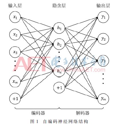
In this paper, the encoder of the self-encoded neural network is used to encode the input data. The output data of the hidden layer is called the encoding of the original data; the encoded data is decoded by the decoder of the self-encoded neural network, thereby recovering the data. Raw input data. Referring to the self-encoded neural network structure shown in Fig. 1, the forward calculation process of the self-encoding neural network is introduced. First, the output of n neurons in the hidden layer is calculated as in equation (1):
The output of m neurons in the output layer is as in (2):
Through the analysis of network forward calculation formulas (1) and (2), it can be seen that the self-encoding neural network processes information from the input layer, through the hidden layer until the output layer output, each layer The calculations between neurons have independence and parallelism; the calculations of equations (1) and (2) include multiplication and addition operations and excitation function operations, and both are performed in sequence.
2FPGA design plan
This chapter analyzes the design requirements of the FPGA-based hardware decoding system, introduces the hardware architecture design of the entire system, the system working principle, and finally describes the design of the network computing module in detail.
2.1 System Analysis
This article designs and implements the decoder part of the self-encoded neural network shown in Fig. 1 in the FPGA, thereby realizing the data decoding function. The self-encoded neural network is trained at the software end. After the network model is obtained, the data normalized by the most common single-byte encoded ASCII code will be input to the encoder of the self-encoded neural network to obtain the encoded data, and the encoded data will be finally encoded. The data is sent to the FPGA side for data decoding to restore the original input ASCII code.
By analyzing the forward computation of the self-encoding neural network, the calculation process includes multiplication and addition operations and excitation function operations. The calculations between each neuron in each layer of the network are independent and parallel. In the process of decoding the encoded data, the designed hardware system is required to have real-time characteristics. FPGA as a distributed parallel processing system, which contains a large number of logical units and computing units, and has the characteristics of programmable, fast, high flexibility, easy configuration, short design cycle, so this paper selects FPGA as the designed data decoder Hardware implementation platform.
The designed decoder is the hidden layer to output layer part of the self-encoded neural network shown in Fig. 1. It contains n × m weight parameters, m offset parameters, and n and m denote network implicit respectively. The number of layers and output layer neurons. Since the decoding function requires only the forward calculation of the network, the weights and biases of the network are fixed values. Therefore, in the design, the FPGA internal resources can be used to store the network weights and offsets and participate in the network in the form of fixed values. Operation.
A complete decoding process of the decoder can be briefly described as: input data → decoding calculation → output result. In practical applications, multiple sets of encoded data are often included, so the encoded data is stored in an external memory in the design for reading by the FPGA. SD memory card is a new-generation memory device based on semiconductor flash memory. It is widely used in portable devices due to its small size, fast data transmission, and hot plugging and other excellent features [13]. So this design chooses to use SD card to store encoded data. The SD card reading operation reads data of one sector at a time, and the number of input data of the network calculation module is the same as the number of hidden layer neurons shown in FIG. 1, and the two data amounts do not match. In addition, SD card read data operations and network calculations are in an asynchronous relationship. Therefore, this design incorporates a FIFO module as a data buffer between the two asynchronous modules of the SD card reading data module and the network computing module. This design is also easily extended to The network structure of other different neuron numbers.
In addition, in order to facilitate manual control of decoding multiple sets of encoded data, a key signal is used in the system design to generate a start signal for a decoding operation. The design is based on the ASCII code encoding and decoding of the system for testing, so the design uses the industrial character LCD display special decoding letters, numbers, symbols and other display decoding results. Finally, in order to increase the stability of the FPGA hardware system and reduce the jitter and tilt of the system clock, a mixed-mode clock manager (MMCM) is added in the design to generate a difference in the case of a set phase and frequency relationship with the input clock signal. The clock signal that is used for each module operation.
2.2 Hardware System Architecture
Based on the above analysis, the hardware architecture of the designed FPGA is shown in Figure 2. The system peripheral modules include an SD card that stores encoded data, a crystal oscillator that generates a differential clock signal, keys that generate a reset signal and control system operation, and an LCD1602 display that displays network calculation results. The FPGA contains three major modules, namely: data loading module, data processing module, and mixed-mode clock manager.
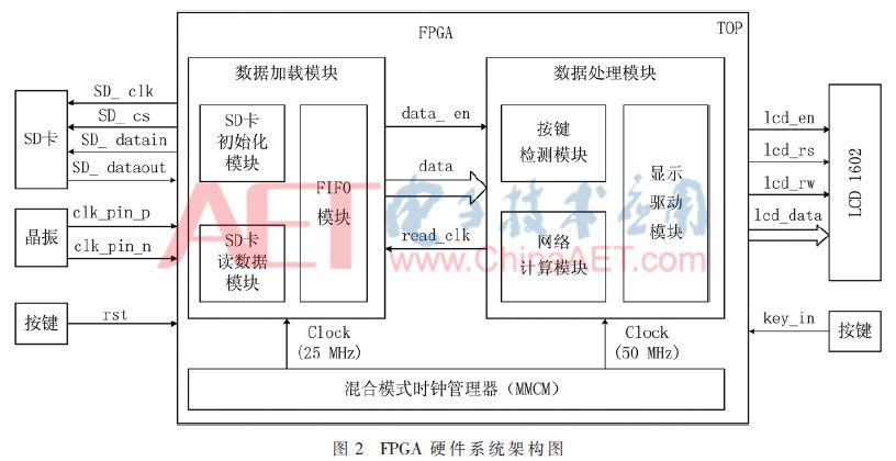
The SD card is used to store the encoded data in the design. A simple command/response protocol [13] is used to operate the SD card. All commands are initiated by the FPGA. The SD card returns the response data after receiving the command. To read the data in the SD card, it is necessary to first complete the initialization of the SD card. The system design the SD card initialization module and the SD card read data module according to the function respectively, which conforms to the design principle of FPGA modularization. The FIFO module serves as a data buffer between the SD card and the network computing module, and is also used for asynchronous data transmission. Therefore, an independent read clock and write clock are used in the design for asynchronous operation.
The key detection module constantly reads the value of the external key output signal key_in. When a key depression is detected, the module generates a high pulse signal, which is used as the starting signal for a decoding operation. The network computing module calculates the read data according to the calculation method of the neural network. The display driver module design adopts a finite state machine to control the initialization and data display operations of the LCD1602. The module has a signal line connection with the network calculation module to implement the calculation result to the display driver module. The display driver module controls the LCD1602 pair. Calculation results are displayed.
In the hardware architecture diagram shown in FIG. 2 , the mixed-mode clock manager divides the external clock to generate the clock signals required for each module to work, and it is connected to the data loading module and the data processing module via two clock lines, respectively. The load module and the data processing module are connected through 3 signals of data_en, data, and read_clk.
2.3 System Working Principle
The characteristic of FPGA is that it can realize parallel operation. In the system architecture diagram shown in Figure 2, the data load module and data processing module work in parallel and asynchronously.
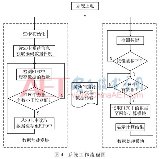
Data Loading Module: After the system is powered on, the data loading module first controls the SD card initialization module to initialize the SD card. The initialization operation includes a series of commands. After the initialization is completed, the SD card initialization module outputs an initialization completion signal. Since the encoded data in the SD card is written on the PC side in the form of a FAT32 file system, after the initialization of the SD card is completed, the data loading module controls the SD card reading data module to read the FAT32 file system information in the SD card. Get the length of the encoded data, which is the number of bytes contained in the file, which will be used to control the reading of encoded data. Finally, the data loading module continuously detects the amount of buffered data in the FIFO. When the amount of data is less than the set value, the SD card reading data module is controlled to read the encoded data in the SD card into the FIFO for buffering.
Data processing module: When the key detection module detects that an external key is pressed, it will generate a high pulse signal, and then the data processing module will read data from the FIFO through the data_en, data and read_clk 3 signals to the network calculation module for calculation. Then, the calculation result is displayed on the external LCD 1602 through the display driving module control. The timing relationship between the data_en, data, and read_clk signals between the data load module and the data processing module is shown in FIG. 3 . When data_en is high, data representing valid data in the FIFO can be read, at this time every time the read_clk signal is read. When the rising edge arrives, one data can be read from the data port.
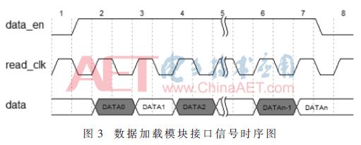
Figure 4 shows the work flow diagram of the FPGA hardware system, in which the SD card read operation and the network calculation are in an asynchronous relationship. The FIFO module added in the system is used as an SD card read data module and a network calculation module between two asynchronous modules Data buffer.
2.4 Network Computing Module Design
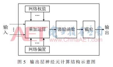
The network computing module is the core module in this design. It is used to implement the decoder in Figure 1, and the weights and offsets of the coded data and decoder parts are multiplied and added according to equation (2), and the output is obtained through the excitation function. value.
It can be known from the network forward calculation analysis that it includes multiplication and addition operations and excitation function operations. Since the input of the self-encoding neural network in this design is the normalized data of the ASCII code, that is, the original ASCII code value is divided by 128, the output value of the excitation function in the FPGA module needs to be increased by 128 times. The ASCII value. Since 128=27, multiplication operation in FPGA can be implemented by shifting, so expanding the calculation result by 128 times is equivalent to shifting the decimal point in binary format right by 7 bits. Furthermore, 7 bits directly after the decimal point is cut is the ASCII code value after the calculation result is expanded 128 times. Therefore, the network computing module divides the calculation into three parts: multiplication and addition operation, excitation function operation, and truncation operation. As shown in FIG. 5, a schematic diagram of the calculation structure of an output layer neuron is shown in FIG. 5. Each neuron in the output layer is shown in FIG. 5. The computational structure is calculated in a parallel, independent manner.
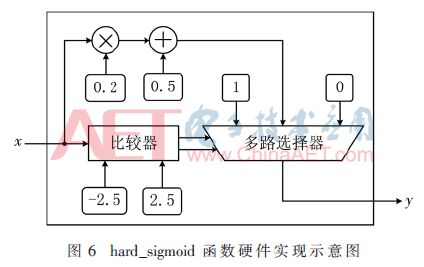
The multiplication and addition operation in the module is to calculate the coded data, decoder weights and offsets according to the multiplication and addition rule in the excitation function in equation (2). The excitation function of this design output layer neuron is hard_sigmoid function [12], and the expression is formula (3):

According to the definition, the hard_sigmoid function is a piecewise function, and each segment has a linear relationship, which is very easy to implement in the FPGA system, that is, using the conditional judgment statement to judge the input and output different values, as shown in FIG. 6 as the hard_sigmoid function. Hardware implementation diagram.
3 system test analysis
In order to test the implementation of the self-encoded neural network designed on the FPGA platform, the network structure chosen in this paper is that the input layer and output layer contain 4 neuron nodes, and the hidden layer contains 8 neuron nodes. The selected application background is the encoding and decoding of ASCII code, in which the software side completes the encoding of the ASCII code, and the resulting encoded data is decoded at the FPGA side.
The experimental test set is generated by software. Under the software environment, the non-control characters in the ASCII code (code values ​​32-127, a total of 96) are normalized, and then input into the design in groups of 4 in a random combination. The self-encoded neural network obtains the output of the hidden layer and stores the output as the test input data of the FPGA in the SD card. The selected FPGA hardware platform is the Xilinx VC707 FPGA development board. The system development environment is Xilinx ISE 14.7, and the simulation environment is ModelSim SE 10.1c. Figure 7 shows the hardware system test chart.
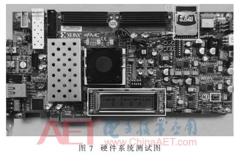
In the hardware system test chart shown in Figure 7, 1 is an SD card, 2 is a LCD 1602 display, and 3 is a control button. After the system is powered on, the data is read continuously from the SD card through the press of the control button. After calculation by the network calculation module, the result is displayed on the LCD1602 display, displaying 4 characters at a time, as shown in the LCD1602 display in Figure 7. The second row is the decoded 4 data, corresponding to the 4 outputs of the neural network shown in FIG.
3.1 Network Calculation Results Analysis
The neural network is trained to obtain a set of optimal parameters, including network weights and offsets. In order to implement the decoder part of the designed self-coding neural network in the FPGA, it is necessary to acquire the data (the output data of the hidden layer of the neural network) encoded by the ASCII code and the network weights and offsets of the decoder part. In addition, since the FPGA can only recognize and calculate binary data, it is necessary to convert the above data into binary data.
In FPGA design, the representation of data is directly related to the consumption of FPGA logic resources. The more data bits represent the higher the data precision, the more logic resources are consumed. Therefore, FPGA design needs to weigh the relationship between FPGA resource consumption and data accuracy. In combination with the practical application of this article, and in order to better balance the accuracy, resource consumption, and power consumption in the FPGA design, this design uses fixed-point numbers to represent the above data.
Since the finite-bit fixed-point number is used to represent data in the FPGA design, the original data may be subject to error due to truncation of the data during the fixed-point quantization process. According to the design of the network computing module, the output is 7 bits after the binary point of the calculation result. Therefore, it is necessary to ensure that the 7-bit data is correct in the design. That is, compared with the original input data, the output error after decoding needs to be less than 2-7. That should be less than 7.812 5×10⁻³. This article uses the Fixed Point Toolbox under MATLAB to quantify the data, and then analyzes the impact of the data's different quantization bits on the calculation result error. Figure 8 shows the fixed-point number representing the number of decimal places and the maximum error. Relationship.
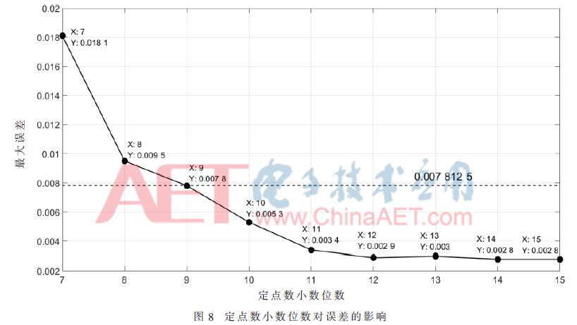
As can be seen from Figure 8,
(1) As the number of fixed-point decimal places increases, the maximum error value continuously decreases, that is, the data accuracy becomes higher and higher;
(2) After the fixed-point decimal place becomes 12 bits, its maximum error remains basically unchanged;
(3) When the fixed-point decimal place is 9 bits, its maximum error is basically the same as 7.812 5×10⁻³; when the fixed-point decimal place is 10 bits, its maximum error has already met the requirement of less than 7.812 5×10⁻³.
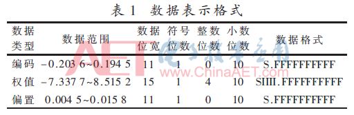
Based on the analysis results shown in Fig. 8, when designing the network weights, offsets, and coded data in the design for fixed point quantification, the decimal places are all designed to be 10 bits. The number of integer bits can be further determined by analyzing the network's weight, offset, and size range of the encoded data. Table 3 shows the binary fixed-point number formats for the three types of data.
This design simulates the network computing module in the ModelSim environment, and compares the calculation results of the module output with the original input data in the software. The absolute value of the absolute error in the tested data is less than 7.812 5×10⁻³. Design error requirements. In addition, through hardware measurement, all encoded data are correctly decoded after being calculated by the FPGA, and the results are displayed on the LCD1602. That is, the designed FPGA hardware system performs the decoding function correctly, thereby verifying the design of the network calculation. Module error analysis.
3.2 System Performance Analysis
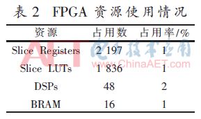
Table 2 shows the main resources used by Xilinx ISE after system engineering is implemented. It can be seen that DSP resources occupy a large amount, the main reason is that the multiplication and addition calculations and the excitation function operations in the network computing module all contain fixed-point multiplication and addition operations, thus occupying more DSP resources. In addition, the occupation of BRAM resources mainly comes from the implementation of the FIFO module and the storage of network weights and offsets in the network computing module.
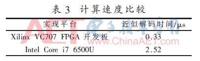
As shown in Table 3, FPGA hardware is used to achieve data decoding speed and software decoding speed. Software decoding is achieved in MATLAB software. The CPU is an Intel Core i7 clocked at 2.5 GHz. FPGA hardware decoding speed is calculated by setting a counter in the FPGA, counting the clock from reading the input data of the decoder to the final output result, and then using the ChipScope tool to check the count value to calculate the working time. The results in Table 3 show that the FPGA hardware decoder designed in this paper is more than 7 times faster than the CPU software decoding.
Through the XPower tool provided by Xilinx ISE, the running power of the FPGA can be roughly 0.389 W. The power consumption of the LCD1602 in the peripheral devices of the designed system is approximately 0.693 W. The power consumption of other peripherals is negligible, so the total power of the entire system is The consumption is about 1 W. In contrast, the Intel Core i7-6500U CPU with a 2.5 GHz frequency can consume as much as 65 W. This shows that the system consumes only 1.5% of the power of a general-purpose CPU, making it particularly suitable for the FPGA-based design of this article. The decoder is used in low-power portable devices.
4 Conclusion
Using the mapping relationship between the input and output of the neural network, data encoding and decoding can be realized simply and efficiently. Based on the structure and characteristics of the self-encoding neural network, this paper uses it for encoding and decoding, and implements the decoder part of the self-encoded neural network in the FPGA. Through the analysis of the design of the software algorithm and the network calculation process, the FPGA module is designed according to the functions and requirements. Using ModelSim software to simulate the design of each FPGA module, the use of Xilinx ISE design, synthesis and implementation of the entire project, and download the programming file to the Xilinx VC707 FPGA development board for verification, while the resource consumption of the FPGA system, Calculate speed and power consumption for evaluation. Through testing, the encoded data in the software can be correctly decoded in the FPGA system. At the same time, compared to the general-purpose CPU, the system's calculation process is accelerated by more than 7 times, while the operating power consumption is only 1.5% of the CPU, so it has the characteristics of high speed and low power consumption. It is especially suitable for real-time performance and low power. Consumption in portable devices.
RandM Tornado 9000 is a new Disposable Vape device It contains 18ml 5% nic salt e-juice and vape up to 9000 puffs. It's recharge, The rechargeable port at the bottom of the device guaranteeing you finish the last drop of the ejuice in the tank all the time. The price of the randm tornado 9000 is very good price, if you want to buy randm tornado 9000 near me, please contact us.
Tornado 9000 Puffs, RandM 9000, Randm Tornado 9000, 9000 puff disposable, 9000 Puffs vape
Shenzhen Kate Technology Co., Ltd. , http://www.katevape.com