Digital Radio Frequency Memory (DRFM) is a microwave signal storage system used to implement RF signal storage and forwarding functions. The digital radio frequency memory carries out high-speed sampling, storage, transformation processing and reconstruction of the received radio frequency signals, and realizes high-speed signal acquisition and preservation, diversity of interference technologies, and control flexibility. Digital RF memory has become a key component of the electronic countermeasures system.
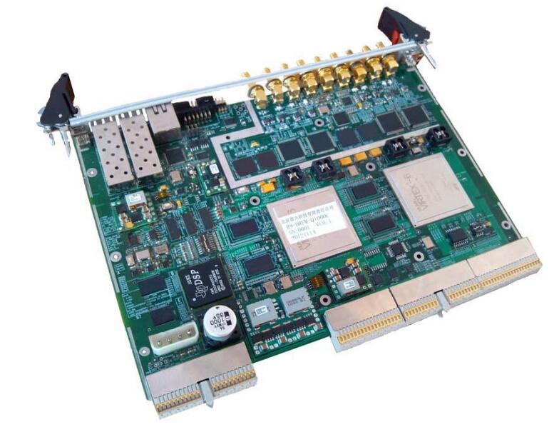
The basic working principle of digital radio frequency storage (DRFM): First, the input RF signal is down-converted into an intermediate frequency signal, which is converted into a digital signal after A/D conversion and written into high-speed memory. When it is necessary to retransmit this signal, the digital signal is read out under the control of the controller and converted into an analog signal by D/A. Then use the same oscillator for up-conversion to obtain the RF output signal and complete the store and transfer of the input signal.
First of all, the quantization process is analyzed. It is assumed that the baseband input signal is a sinusoidal signal gi(t)=Esinωit and the number of quantization bits is N. The quantized signal can be represented by a staircase wave y(t), and y(t) can be considered as It is a superposition of N pairs of rectangular waves. If the number of quantization bits of the A/D conversion is m, then the number of quantization steps in the positive or negative half cycle is N=2m-1. The expression of the staircase wave is:
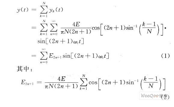
E2n+1 is the amplitude of the quantized harmonic components. The power of each harmonic can be calculated by this formula.
In the process of sampling, for the sake of simplicity, one quantized signal is taken as input, and the input signal is:

Where: E, ωi are the amplitude and angular frequency of the input signal, respectively. Let the sampling pulse signal be fs(t) and the sampled signal be fo(t). The mathematical expression of the sampling process in the time domain is fo(t)=fi(t)fs(t), which is used in DRFM. Equidistance uniform sampling, sampling period Ts, sampling clock frequency ωs = 2πfs. In an actual circuit, sampling is completed at the instant that the sampling pulse rises. Therefore, the width of the sampling pulse can be seen as a narrow pulse width, using τs. To represent. The Fourier series of sampling pulses is:

Where: Es, τs, Ts, and ωs are the amplitude, pulse width, period, and angular frequency of the sampled signal, respectively. then:
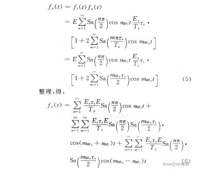
In equation (6), the first term is the baseband harmonic signal, which is the spectral component produced by quantization. Only in the baseband filter, the harmonics will become spurious, and all nωi â€Ï‰s/2 terms will be Filtering (n takes an odd number); the second term is completely outside the filter and does not need to be considered; the third term is an intermodulation signal that satisfies (mωs-nωi) all the components of ωs/2 and will become an intermodulation spurious signal, They are caused by the cross-modulation of signal harmonics and clock harmonics. If the duty cycle of the pulse signal is represented by D, and the second term is ignored, then equation (6) becomes:
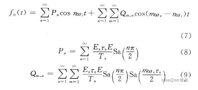
Equations (8) and (9) are methods for calculating the higher harmonics and amplitude of the intermodulation signal for the 1 dB quantized DRFM.
Digital RF Memory Block DiagramAs shown in the figure below, the digital RF memory can convert the received signal to an intermediate frequency (IF) signal. Then the bandwidth of the IF signal is digitized. The digitized signal is stored in memory and transmitted to the computer. The computer performs the necessary analysis and correction of the signal to meet the interference technology requirements.
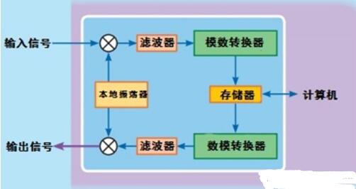
The corrected digital signal is then converted to an analog RF signal. By using the same local oscillator as the initial frequency conversion, this signal is frequently converted to the receiving frequency. In down-converting and up-converting, the unique oscillator keeps the phase of the signal coherent.
The digital RF memory can digitize the received signal, and the digital signal is transmitted to the computer. The computer corrects it and continuously generates a new forwarding correction signal.
The key device of digital RF memory is an analog-to-digital converter. Analog-to-digital converters can be band-digitalized at 2.5 samples per hertz, which can output I&Q (synchronous and quadrature) digital signals. In this way, the phase of the digitized signal can be grasped.
It should be noted that because the digital RF memory will reconstruct the signal, 2.5 samples per Hertz are much larger than the Nyquist rate of 2 samples per Hertz of the digitized receiver. Digitized signals typically have several bits per sample size, although 1-bit digitized samples or phase-only digitized samples are sometimes used.
The computer analyzes the input signal to determine the modulation characteristics and parameters of the signal. The computer usually analyzes the first pulse received by the system and generates a burst of the same or different modulation parameters (systematic). A digital-to-analog converter generates a radio frequency output signal that is a lot larger than the output signal generated by the analog-to-digital converter, which can ensure that the signal quality does not decrease when the radio frequency signal is reconstructed.
Wideband Digital RF Memory Block DiagramA wideband digital radio frequency memory can digitize an intermediate frequency broadband including multiple signals. The jammer system covers the frequency range of the threat signal and outputs the bandwidth of the IF signal that the digital RF memory can handle.
As shown in the figure below, phase coherence is maintained by using a system-unique local oscillator, followed by frequency conversion and subsequent receive signal recovery. The bandwidth of digital RF memory is limited by the sampling rate of the analog-to-digital converter. There are multiple signals in the bandwidth, and attention needs to be paid to the spurious-free dynamic range.
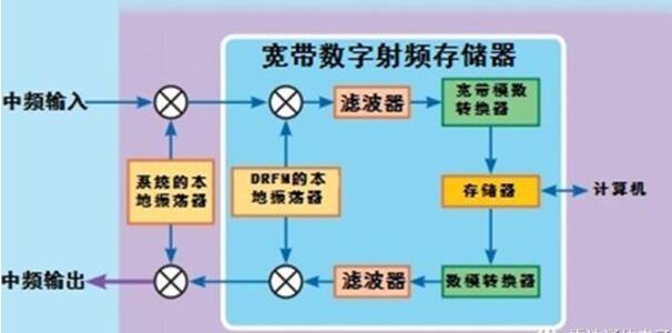
Therefore, analog-to-digital converters need to digitize the maximum available amount of bits. Broadband digital RF memory performance is very satisfactory because they can handle wideband modulation and frequency agile threat signals. There is a bottleneck in the technological level of analog-to-digital converters. Wideband digital RF memory can handle frequency ranges that contain multiple signals.
Narrowband digital RF memory block diagramNarrow-band digital RF memory requires only a bandwidth wide enough to handle the widest bandwidth signal transmitted by the jammer. This means that a narrowband digital RF memory can use a state-of-the-art analog-to-digital converter.
As shown in the figure below, the jammer system converts the frequency range of interest into a frequency range covered by multiple narrowband digital RF memories. The digital RF memory system's input signal is automatically assigned to each digital RF memory.
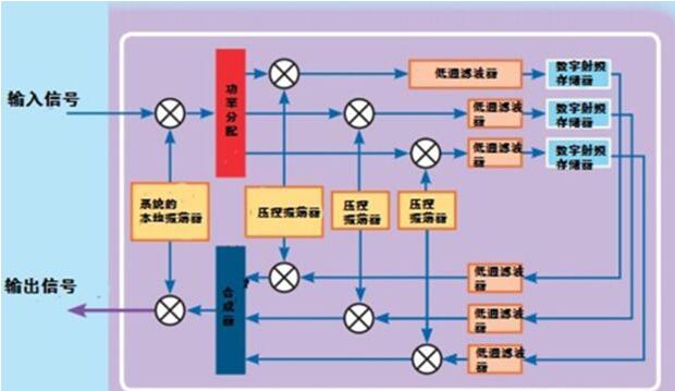
Each digital RF memory handles a different signal and plays its role in supporting interference actions. Then, the analog RF output of the digital RF memory will be synthesized, converted (coherent) and restored to the original frequency range.
It should be emphasized that there is very little spurious response in narrowband digital RF memories because each digital RF memory only processes one signal. Each narrowband digital RF memory handles only one signal. In a multi-signal environment, multiple narrow-band digital RF memories are required for processing.
Digital RF memory functionDigital RF memory is particularly effective when jamming pulse compression radars. Radar achieves pulse compression through linear FM and Barker codes, which can improve the radar's range resolution.
Linear frequency modulation frequency modulates each transmitted pulse. In radar receivers, the compression filtering time can be compressed to a small fraction of the transmitted pulse width before signal processing. If the interference signal emitted by the jammer is not used for such frequency modulation, the effective signal to interference ratio will be reduced by the compression factor. The digital RF memory emits chirped interference pulses to maintain the overall signal to interference ratio.
Barcode compression refers to the binary phase shift keying (BPSK) modulation of each signal pulse in the coding mode. The upper phase shifter and tapped delay line are switched to compress the received pulse length to one symbol. Since the pulse compression cannot be performed without the interference pulse using the Barker code, the effective interference ratio will decrease as the number of symbols increases. The digital RF memory emits interference pulses through the correct Barker code, which maintains the overall signal to interference ratio.
Digital RF memory can also emit coherent interference signals and can occupy a single channel in a pulse Doppler radar processor. This can make pulsed Doppler radar unable to distinguish interfering signal pulses in multiple Doppler channels.
When people talk about 7inch tablet, kids appears on their minds, especially for elementary students or kindergarten kids for playing intelligent exploitation games or online learning. Clients usually choose 7 inch tablet wifi only as 7 inch educational tablet for project, wifi one is much cheaper. Of course, 7 inch Android Tablet with 3G lite or 4G lite also optional. You can always see a right tablet at this store, no matter amazon 7 inch tablet, 8 inch android tablet, or 10.1 android tablet.
Except android tablet and window tablet, there are Education Laptop, Mini PC , All In One PC, which are is the main series at this store. Any other special configuration interest, just email or call us, you will receiving value information in 1-2 working days.
To meet clients` changing requirements, we contributes 10-20% profit to develop new designs according market research and client`s feedback.
So you are always welcome if can share your special demand or your clients opinion for the products.
7 Inch Tablet,7 Inch Android Tablet,Amazon 7 Inch Tablet,7 Inch Tablet Wifi Only,7 Inch Educational Tablet
Henan Shuyi Electronics Co., Ltd. , https://www.shuyiaiopc.com