Abstract: With the increase in the cost performance of high-power LEDs, the increase in output light flow makes it possible to use LEDs in automotive headlamps. The input voltage is changed between 10 and 14 V, and the load is determined by eight 700 mA high-power white LEDs. The driving mode, topology and dimming mode are determined. A constant current LED based on LTC3783 chip PWM control LED brightness is designed. The car headlight drive circuit was simulated with the LTspiceIV software. The results show that the output current is a 710 mA average when the input voltage changes from 10 to 14 V, with a current of 0.7% ripple, current accuracy of 2.1%, output voltage of 28.6 V, and output power of 20 W, the circuit conversion efficiency is 91%. When there is a PWM signal input, the circuit outputs a current with the same duty cycle as the PWM signal. The LED brightness is controlled by adjusting the duty cycle of the PWM signal.
Keywords: car headlights: high power LED; pulse width modulation: LTSPiceIV
0 Introduction Statistics show that 90% of traffic accidents are caused by human factors. The dangers come from complex traffic conditions, including unreasonable information, lack of information and excessive tension. In order to effectively reduce blind spots, avoid glare, and improve the safety of night driving, some famous automobile companies have proposed the concept of advanced headlight system or adaptive front lighting system (AFS), which is characterized in that the vehicle headlights can actively adjust the illumination light. The axis direction automatically adapts to changes in the night driving environment (including oncoming vehicles, curve slopes, highways, city blocks, etc.). In recent years, the development of high-brightness LEDs has been rapid, and the adoption of high-brightness or ultra-high-brightness LEDs in automotive headlight systems will be a development trend. At present, there are reports of 1 201 m ultra-high brightness LEDs, and 8 ultra-high brightness LEDs can generate light intensity of 10 001 m. In addition to its obvious long life, solid structure and low power consumption, LED light source has its inherent small size, flexible design, fast response and easy control, which makes it suitable for automotive adaptive headlight system. A big potential advantage.
Automotive electrical is powered by a lead-acid battery, typically 12 V, but the actual voltage is constantly changing around 12 V. How to use a low-voltage and constantly changing automotive power supply design A drive circuit with high current accuracy, adjustable brightness, and low power consumption is a key technology for manufacturing LED automotive headlamps. In this paper, a constant current LED car headlight driving circuit based on LTC3783 chip PWM control LED brightness is designed under the condition that the input voltage is the vehicle power supply voltage and the load adopts eight 700 mA high power white LEDs. The output current is stable and the precision is high. The circuit conversion efficiency is high.
1 LED lighting characteristics and drive type selection
1.1 LED illuminating characteristics Since LEDs are essentially illuminating diodes, only the threshold voltage and conduction voltage drop are larger, and its dynamic impedance is relatively small. Smaller voltage changes can cause large current changes. The operating current and the conduction voltage drop are exponentially changed as shown in the following equation: ![]()
Where: Is is the reverse saturation current; If is the forward working current, which refers to the forward current value when the LED is normally illuminated.
The LED is a current-type device, and the luminance of the light is related to the operating current. ![]() . Where: m is approximately equal to 1; K is a proportionality factor. When the current increases, the luminance of the light increases proportionally. In order to maintain the same light output, the LED driver should control the current through the LED, that is, drive the LED with a constant current source.
. Where: m is approximately equal to 1; K is a proportionality factor. When the current increases, the luminance of the light increases proportionally. In order to maintain the same light output, the LED driver should control the current through the LED, that is, drive the LED with a constant current source.
The load in this design uses eight Luxeon models of LXML-PWC1-0120 LEDs in series. The LED specification parameters are shown in Table 1.
This article refers to the address: http://

1.2 Choice of drive type
1.2.1 Drive mode LED drive mode can be divided into constant voltage source drive and constant current source drive. The load driven by the constant voltage source is generally connected in parallel with the LED multi-branch. Each branch must be connected in series with a ballast resistor with a certain resistance. When high current output is required, the conversion efficiency of the circuit is low. Since the LED is a current-type device, even a slight change in voltage can cause a large fluctuation of the current. The constant-voltage source drive will affect the illumination quality and stability of the LED; the constant-current source drive can control the output current to be stable, and the LED illumination quality Well, generally connected in series, only a small resistance detection resistor, the efficiency is relatively high, suitable for automotive headlamp LED driver. When the constant current source is driven in series, generally one LED is connected in parallel with each LED to prevent the LED from being burnt and the whole circuit is opened.
1.2.2 Topology The LED driver circuit can be divided into a linear regulator circuit and a switching converter circuit. Although the linear regulator drive circuit is relatively simple, the power consumption on the chip and the current limiting resistor is relatively large and the efficiency is very low. Switching converter drives are further divided into charge pump drives and inductive drives. The charge pump driver uses a capacitor to pass current from the input to the output. The whole solution does not require an inductor. It has the advantages of small size and simple design, but it can only provide a limited output voltage range. It is not suitable for multiple high-power LEDs. In series. Therefore, an inductive boost driver is used in the design. In the circuit of Figure 1, when the MOSFET M1 is turned on, the inductor current increases, energy storage begins, the LED begins to illuminate, and the freewheeling diode is turned off due to the reverse voltage. When the MOSFET M1 is turned off, the inductor current is reduced, and energy is released to continue to flow through the Schottky diode.
1.2.3 Dimming mode In the automotive headlamp system, the conversion of low beam and high beam can be realized by controlling the brightness of the LED, while adjusting the brightness of the LED in the adaptive headlamp system to match the LED of the LED array at different positions. The illumination can achieve different illumination distances and deflection angles of the illumination beam, and adapt to different road condition information. When the input voltage value fluctuates, the current of the LED also fluctuates. Through current feedback, dimming control can be performed to ensure that the current flowing through the LED does not change. In addition, LED brightness adjustment can also be applied to thermal conditioning circuits instead of traditional bulky heat sink devices. The ability to accurately and efficiently implement LED dimming is also an important factor in drive circuit considerations.

In general, techniques such as external SET resistors, linear adjustment, and PWM regulation can be used to control the brightness of the LEDs. The lack of flexibility in the use of SET resistors outside of the LED driver makes dynamic adjustments impossible. Linear adjustment dynamically controls the brightness of the LED, but reduces the efficiency of the LED and causes the color shift of the white LED toward the yellow spectrum. In comparison, the advantages of PWM regulation technology are very obvious. When the PWM pulse is active high or low, the LED input current is maximum or 0, and its on-time is controlled by the duty of the PWM pin input pulse. ratio. Since the LED is always operating under the same current conditions, by applying a PWM signal to control the brightness of the LED, dynamic adjustment of the brightness of the LED can be achieved without changing the color.
In order to ensure that the PWM dimming is not perceived by the human eye, the PWM dimming frequency is generally greater than 100 Hz, but too high a frequency will increase the dynamic loss of the MOSFET. In this design, the PWM dimming frequency is 120 Hz.
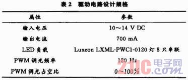
1.2.4 Design Specifications Table 2 shows the design specifications of the LED constant current drive circuit.

2 drive main circuit design
2.1 Circuit composition The circuit is mainly composed of LTC3783, MOSFET tube M1, M2, inductor L1, freewheeling diode D9, sense resistor R9, output capacitor C4 high-power LED string composed of boost-type inductive current control mode drive circuit. The main circuit is shown in Figure 2. The LTC3783 is a high-power LED driver for the current-mode multi-topology converter PWM dimming range from Linear Technology, covering high-voltage LED arrays, backlighting in telecom, automotive and industrial control systems. Stabilizer.

The frequency of the high-frequency control signal f of the chip is determined by changing the size of the external resistor of the FREQ pin of the chip. The GATE pin outputs a pulse signal with a peak value of 7 V, which is the PWM control pulse received by the PWMIN pin and the high-frequency control of the chip LTC3783. The sum of the output pulses. The GATE pin drives the MOSFET M1 to control the on and off of the power MOSFET M1, causing a change in the current flowing through the inductor L1, producing a voltage drop whose sum with the input voltage is the output voltage. The PWMOUT pin outputs a PWM control pulse signal identical to the PWMIN pin, driving the MOSFET M2. The duty cycle of the PWM pulse determines the duty cycle of the LED string current, which in turn controls the brightness of the LED string. The FBN pin receives the voltage signal fed back by the sense resistor R9. When the output current changes due to the input voltage, the duty cycle of the circuit is adjusted to keep the output current constant.
2.2 Calculation of main parameters
2.2.1 Selection of switching frequency f The PWM control pulse signal and the chip high-frequency switch control signal are shown in Figure 3. It can be seen that the two have the following relationship: 

When using PWM to control the brightness of the LED, in order to avoid people's awareness, the frequency of the control pulse is selected as fPWM=120 Hz. Each control pulse high level must contain at least 2 chip high frequency switching pulses, ie N>2. In order to achieve a DIFI of 1:3 000 dimming ratio for digitalization, the chip frequency f is selected to be 1 MHz. The chip switching frequency is determined by the resistor R2 connected to the chip FREQ. The relationship between f and R2 is shown in Figure 4. In this design, R2 = 6 kΩ is selected.
2.2.2 Calculating Circuit Duty D
The formula for calculating the maximum duty cycle of the circuit is ![]()
Where: VOUT is the output voltage; VIN(MIN) is the minimum input voltage; VD is the forward voltage drop V of diode D4. The minimum input voltage is 10 V, the output voltage is 28.6 V, the diode forward voltage drop is 0.4 V, and the maximum duty cycle calculated by Equation (3) is 59%. The maximum duty cycle allowed by the LTC3783 can reach 90%.
2.2.3 Calculating the Maximum Input Current The purpose of calculating the maximum input current is to calculate the rating of other components. The input current is calculated as: ![]()
Where: χ/2 represents the ratio of ripple current to average current. Here χ = Iout × 20% = 700 mA; DMAX is 59%; the maximum input current is 1.8 A.
2.2.4 Calculation of Input Inductance L1 The ripple current through inductor L1 is: 
Calculated L = 12μH.
2.2.5 Calculation of Output Capacitor C4 The output capacitor is mainly to reduce the ripple of the output current. The ripple of the current flowing through the LED has an important influence on the light efficiency and light decay of the LED. Under a certain average current, the larger the ripple, the larger the effective value, the more heat is converted, the lower the light effect, the light decay The more powerful, the shorter the life. Therefore, for LEDs, the better drive current is a DC current with a small ripple.
Assuming the ripple voltage does not exceed 1% of the output voltage, there are: ![]()
The larger the capacitance, the smaller the ripple current. Considering the cost factor, the minimum output capacitance calculated by equation (7) is 5 μF. To prevent excessive heat generation, the output capacitor should be a low-ESR, high-withstand ceramic capacitor.
3 MOSFET tube, freewheeling diode selection MOSFET tube leakage terminal voltage is the output voltage is equal to 28.6 V, assuming that the drain peak voltage is calculated by 30% higher than the rated voltage, then the maximum voltage of the MOSFET tube drain is 38 V . The maximum current IIN(MAX) flowing through the MOSFET M1 is 1.8 A, and the maximum current of M2 is about 700 mA. Generally, three times the actual current is selected as the rated current of the MOSFET. Therefore, an N-channel MOSFET with a withstand voltage of 60 V, a maximum forward current of 7.5 A, and an internal resistance of 11 mΩ was selected, model number SI4470EY.
The voltage of D9 is the same as the voltage of MOSFET M1. The maximum voltage is 38 V. The current flowing through D9 is equal to the load output current of 700 mA. Therefore, choose Schott with a withstand voltage of 40 V and a maximum forward current of 1.16 A. Base diode, model number ZETEX ZLLS1000.
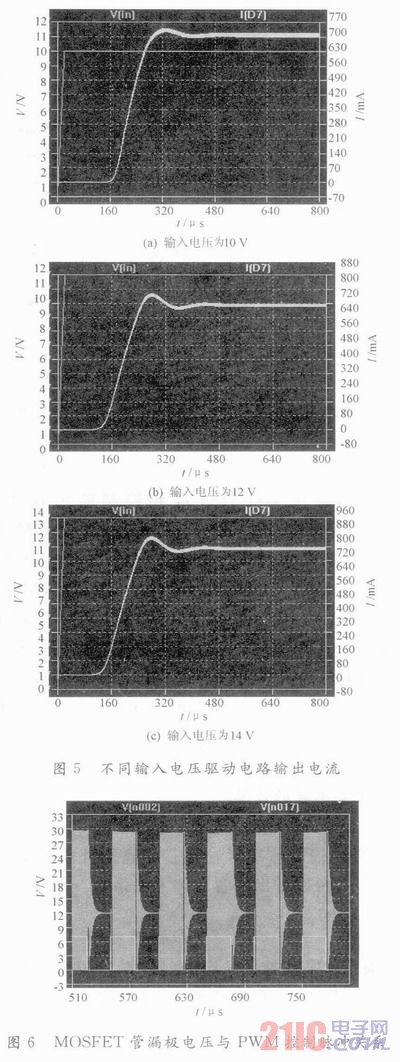
4 Simulation results The circuit was simulated with LTspiceIV software. Figure 5 shows the output current of the load LED as a function of time when the input voltage is 10 V, 12 V, and 14 V, respectively, without PWM dimming. As can be seen from Figure 5, as the input voltage changes, the duty cycle of the circuit changes and the output current remains substantially unchanged. After the current is stable, the measured current changes between 705 and 715 mA, that is, the drive circuit outputs a current of 710 mA with 0.7% ripple current. Current accuracy is: 
Where IOUT(MAX) is the actual output current maximum; IP is the set output current.
Figure 6 is a PWM waveform and MOSFET drain voltage waveform diagram during PWM dimming. It can be seen that the input signal of the power transistor MOSFET is the sum of the PWM output signal and the LTC3783 high frequency switch control output signal, and the duty ratio of both signals is The output current can be adjusted.

Figure 7 shows the actual output current when the control pulse duty cycle is 20%, 50%, and 80%, respectively, during PWM dimming. The actual output current is the same as the duty cycle of the PWM pulse, which in turn enables adjustment of the LED brightness.

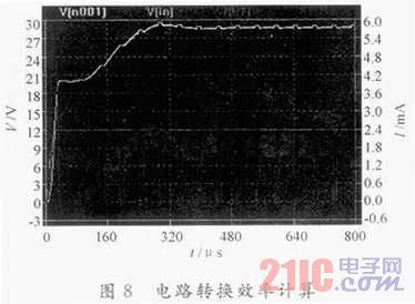
To calculate the conversion efficiency of the circuit, the values ​​of the input voltage, input current, output voltage, and output current of the driving circuit are measured as shown in FIG. It can be seen that the input voltage VIN is 12 V, the input current IIN is 1.86 A, the output voltage VOUT is 28.6 V, and the output current IOUT is 710 mA, so the circuit conversion efficiency is: 

5 Conclusion Based on Linear Technology's LTC3783 chip, this paper designed eight high-power white LED string driver circuits for automotive headlamps. The simulation results show that when the input voltage is 10~14 V, the output current is an average value of 710 mA, with 0.7% ripple current, current accuracy of 2.1%, and output voltage of 28.6 V. The output power is 20 W and the circuit conversion efficiency is 91%. The drive circuit also has a PWM dimming function that outputs a current equal to the duty cycle of the PWM signal. The LED driver circuit designed in this paper has the characteristics of high constant current precision, large output power, high conversion efficiency and adjustable brightness.
The telecom parts are metal or plastic equipment which is used for the purposes of telecommunication, like as telecom equipments and IT hardware: LSA Module, Krone Module, Disconnection Module, Distribution box, Label holder, Test plug, Wiring block, Rack screws
When you buy from Uonicore Electronics, you get quality telecoms equipment, good lead times, original parts and continued support for legacy equipment. In addition, you can support your environmental credentials with our recycling options and use of refurbished equipment.
Telecom Parts,telecommunication parts,telecom components,Server Rack Mount Screws
NINGBO UONICORE ELECTRONICS CO., LTD , https://www.uonicore.com