Analog system designers face many design challenges. Not only do they need to select the right integrated circuit (IC) devices, they must also accurately predict the interaction of these components within the system. From this point of view, the design of analog-to-digital (A/D) converters is a daunting challenge because various input sampling structures must be considered at the system level and the correct choice must be made. This article will explore several common input sampling structures and discuss the impact of each structure on other parts of the system.
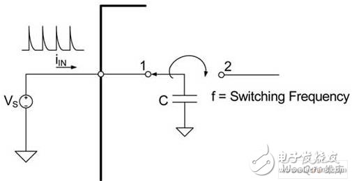
Input sampling basic circuit structureWith the popularization of digitization and the development of technology, the application of A/D converters is ubiquitous. Among the many CMOS A/D converters currently in use, one common solution is to use a switched capacitor structure for input sampling. In this most basic configuration, the input section consists of a relatively small capacitor and an analog switch. As shown in Figure 1, when the switch is set to position 1, it enters the sampling process and the sampling capacitor is charged to the sample. The voltage of the node (VS in this example). Then, the switch is switched to position 2 to switch to the discharge process where the charge accumulated on the sampling capacitor is discharged or transferred to other circuits of the sampling circuit. Charging, then discharging, recharging, and discharging, this process is repeated.
In the above circuit structure, no buffer is used, but switched capacitor input is used directly, which causes serious system-level problems. Because during the sampling process, the current required to charge the sampling capacitor to the sample point voltage must be provided by an external circuit connected to the A/D converter input. When the capacitor is switched to the sampling node (switch position 1 in Figure 1), a large current is required to rapidly charge the capacitor. In fact, the magnitude of this transient current is a function of the sampling capacitor value, the capacitance switching frequency, and the sampling node voltage.
The switch current is represented by the following equation: iin = CVf, where C is the capacitance of the sampling capacitor, V is the voltage at the sampling node (VS in this example), and f is the switching frequency of the sampling switch. This switching current will produce a higher peak current overshoot at the sampling node (as shown in Figure 1).

Figure 1 Simple Switched Capacitor Input Structure
When designing the front-end analog circuit of the A/D converter, it is necessary to consider the adverse effect of this switching current. When this current flows through any resistor, a voltage drop is generated, resulting in a voltage error at the sampling node of the A/D converter. If the input of the converter is connected to a high-impedance sensor or a high-impedance filter, the error will become very large.
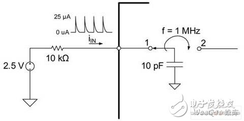
For the sake of detailed explanation, an example is cited, as shown in FIG. 2 . In this example, it is assumed that the front end of the A/D converter is provided with a resistor with a resistance of 10 kΩ to isolate the sensor and improve the electrostatic discharge (ESD) protection function.

Figure 2: Unbuffered switched capacitor input with series resistor
In this example, the sampling capacitor is 10 pF and the switching frequency is 1 MHz. According to the above equation, the transient current is about 25 μA. When this transient current passes through the 10 kΩ resistor in series with the input, a voltage error of 250 mV will occur at the sampling node. This is the worst case estimate since the sample point may stabilize before the next sample period. The settling time of a specific charge loop depends on the RC time constant formed by the 10 kΩ resistor and the sampling capacitor and the parasitic capacitance at the input of the A/D converter. Parasitic capacitance comes from the A/D converter's connection lead, board trace length, and internal MOS switch capacitance. In addition, an external buffer circuit may be required to provide the necessary current and ensure that the sampling points are set correctly to maintain linearity. However, at higher switching frequencies, the amplifier output impedance increases. Therefore, careful selection of the amplifier and associated circuitry is required to resolve transient switch current issues.
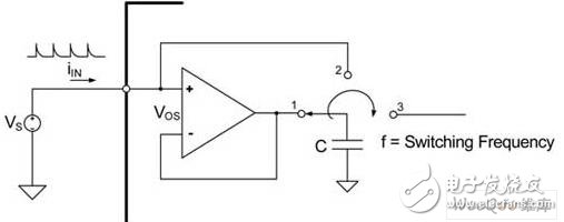
Input sampling improves circuit structureIn order to reduce as much as possible the large charging current that the external circuit must provide, and the adverse effect of the transient current overshoot caused by high-speed switching of the switch, the basic circuit structure shown in FIG. 1 is improved. The improved circuit is shown in Figure 3. By comparison, it can be found that the improved circuit adds an internal buffer before the sampling capacitor.

Figure 3: Buffered switched capacitor input
After the internal buffer is added, the analog switches can be combined into three different states. At position 1, the sampling capacitor is quickly charged to the sampling node voltage (VS) plus or minus (depending on the polarity of the offset voltage) buffer voltage deviation (VOS). At this stage, the transient current required to charge the capacitor is no longer provided by the external circuit, but is provided by the internal buffer circuit. The internal buffer is optimally designed to provide a low output impedance at the required switching frequency to properly charge the capacitor for the specified charge time. Then, reset the switch so that it is connected to position 2 in Figure 3. The sampling capacitor in this stage is directly connected to the sampling node of the A/D converter. The sampling capacitor is then charged or discharged so that the capacitor voltage is equal to the sampling node voltage. There may still be a small amount of switching current, but the required external circuit current is small because the capacitor voltage has been charged to the internal buffer's bias voltage range. The key to this solution is that the pre-charge time at which the switch is set to position 1 must be accurately calculated to avoid this charging time being too long, causing over-charging and back-discharging the external circuit at the input.
Finally, the analog switch is switched to position 3 and the sampled voltage is transferred to the rest of the sampling circuit. This phase is exactly the same as the basic structure shown in Figure 1.
By comparison, the advantage of the switched-capacitor input structure with a buffer circuit is that it can drastically reduce the transient current required for the external circuit of the A/D converter. In the previous example, the sampling capacitor was 10 pF and the switching frequency was 1 MHz. Assume that the internal buffer voltage is biased at 10 mV. After a reasonable control of the precharge time, the transient current generated during the charging phase associated with the external circuit is only 100 nA, which is lower than the unbuffered sampling input transient current. 250 times.
Input buffer further optimizationIn some cases, a fixed or programmable gain amplifier can be integrated into the device at the front of the A/D converter. The integrated amplifier not only helps reduce the switching current that must be provided by external circuitry, but also amplifies the analog signal. In addition, a chopper-stabilized amplifier can be used to reduce 1/f noise, the so-called "flicker noise." This low-frequency noise is caused by the surface state of the MOS transistor channel inherent in the production process. Chopping eliminates 1/f noise and reduces external current requirements. However, due to the mismatch of MOS switches, there will still be a small amount of input transient current in the circuit.
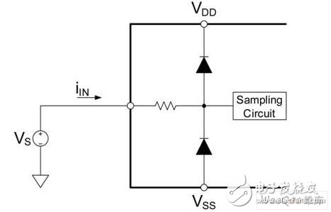
Regardless of the sampling structure, the A/D converter must adopt ESD protection. For CMOS solutions, clamp diodes are generally used to provide ESD protection, as shown in Figure 4. The clamp diode effectively limits the voltage applied to the internal transistor of the converter. If the difference between the input voltage and the power rail exceeds the diode voltage drop (usually 0.7V), the diode will conduct, limiting the voltage. However, the clamp diode also suffers from current leakage and must be considered when designing the analog input circuit. Although this leakage current is usually small, perhaps only a few picoamps, the current will increase dramatically with increasing temperature.

Figure 4: CMOS ESD Protection
in conclusionWith the continuous development of A/D converters, it is becoming more and more important for system designers to fully understand the input structures used and the influence of such structures on external circuits. This article discusses a simple switched-capacitor input structure. Switching current requirements have a huge impact on the overall performance of the system, so external circuits must be properly designed. The integrated buffer or amplifier can greatly reduce the switching current and simplify the external circuit design of the A/D converter. ESD protection circuits also affect external current requirements, and their effects can vary greatly with temperature.
HCOW iTitan 5000puffs disposable vape in stock now
Hcow Ititan 5000Puffs,5000Puffs Disposable ,E-Cigarette ,Disposable Vapor Pen
Shenzhen Kester Technology Co., Ltd , https://www.kesterpuff.com