introduction
This article refers to the address: http://
According to the survey, 4% of the power modules currently in use are used in automotive applications. This market is expected to grow by 20% annually in the next few years. Inverters for hybrid and electric drives have been seen in trucks, buses and agricultural vehicles as well as in automotive and racing applications. Due to the different needs of different application areas, the main focus in all cases is to develop reliable packaging technology for power modules. The most common packaging solutions today are soldered modules with and without substrates, as well as substrateless modules that have recently been sintered. These packaging technologies have different advantages and disadvantages, which is why life-cycle design requirements evaluate these technologies for hybrid and electric vehicle applications. For example, in the cooling water cycle, the changing ambient temperature is the cause of the passive thermal cycle. In addition, the power loss generated in the power semiconductor produces a transient (5-20 s) t = 40 ° C ~ 60 ° C temperature rise. Here, the power semiconductor is heated from a cooling water temperature of 70 ° C to over 110 ° C to 130 ° C, after which they fall back to the cooling water temperature. Since the materials used have different coefficients of thermal expansion, each temperature change causes mechanical stress. This is the cause of material fatigue in the soldering and bonding connections and ultimately leads to component failure.
Avoid soldering connections
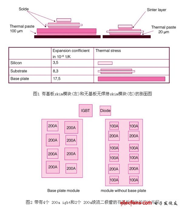
In the substrateless module using crimp technology, there are several ways to improve the reliability of the module. By continually avoiding solder joints, solder fatigue - the main failure mechanism of this power module - can be completely eliminated. Here, the soldered connection on the chip and the insulating dbc ceramic substrate is replaced by a highly stable sintered layer, which is electrically connected by crimping. There are many advantages to removing the substrate: first, the thickness of the thermally conductive coating between the module and the heat sink can be reduced. Thermally conductive coatings are one of the main factors affecting total thermal resistance in power modules, which is why it is necessary to use as thin a thermally conductive coating as possible. In a substrate module, a thermally conductive coating of 75 to 150 μm is required to compensate for the bending of the substrate. In the substrateless module, the main problem to be solved is how to compensate the roughness of the heat sink and the surface of the dbc ceramic substrate, which is why a 20-30 μm thermal conductive coating is sufficient. Removing the substrate means removing a major factor that causes thermal stress.
Solder joint removal eliminates solder fatigue, a common failure mechanism in this power module. Substrate removal also eliminates most of the thermal stress. The accelerated passive thermal shock test at 40 ° C / 125 ° C shows that the temperature conduction stress is effectively reduced, and the reliability is greatly increased: in the case of a substrateless sintered module, the number of possible thermal shocks is increased by 15 times. A further advantage of removing solder interconnects and substrates is that in a substrate module, the area of ​​the soldered dbc substrate should be minimized to reduce fatigue of the solder joint material; here, the high thermal conductivity of the substrate ensures the required heat transfer. In contrast, when designing a substrateless module, the area of ​​the dbc substrate can be larger, as shown in Figure 1.
Optimize heat distribution
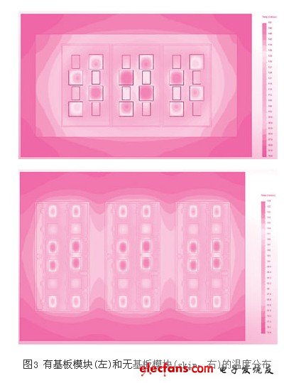
The following section looks at the positioning of igbt and freewheeling diodes in three-phase 400a, 600v inverter modules. In the case of a substrate module, each semiconductor switch uses two 200a igbts and two 200a freewheeling diodes, as shown in Figure 2. Therefore, a complete phase consists of four igbts and four freewheeling diodes. The optimal arrangement for the substrateless module is that each switch has four 100a igbts and two 200a freewheeling diodes (eight igbts and four freewheeling diodes per phase). This means that the base area of ​​the substrateless three-phase module is about 10% larger than that of the substrate module.
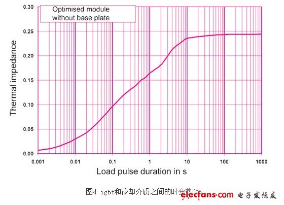
In contrast, the layout of the substrateless skim module with eight 100 aigbts and two freewheeling diodes uses a larger dbc ceramic substrate to optimize heat distribution and heat dissipation. When the inverter is running, conduction and switching losses are generated, which means that the power semiconductor becomes a local heat source. With the help of 3D finite element calculations, the heat propagation in the inverter module and the heat sink for any given operating state can be calculated, as shown in Figure 3. For example, when a hybrid or electric vehicle accelerates, most of the power loss is generated on the igbt, while the freewheeling diode is subjected to a lower load.
Load conditions: battery voltage = 350v, output current = 250a, output voltage = 220v, output frequency = 50hz, switching frequency = 12khz, phase angle cosf = 0.85, cooling medium temperature = 70 °C. This is why the position of igbt appears as a strong heat source in the thermographic image. In the case of a substrate module, heat is concentrated in the center of the three-phase configuration. Due to the tight positioning of the semiconductor and the short distance between the phases, the temperature of the igbt is the highest at this point. Although the freewheeling diode is only subjected to moderate loads during this operating state, igbt causes the freewheeling diode in the center of the module to heat up significantly. In contrast, the diode temperature at the edge of the inverter module is 15 °C lower. Despite the backplane, the temperature of the power semiconductor module in the edge area of ​​the inverter module is much lower than the center of the module, eventually leading to a non-uniform heat distribution of the three phases: the average thermal load of the mesophase igbt is almost equal to the igbt of the two phases on the side The average temperature is 10 °C higher. The highest and lowest values ​​of the igbt temperature differ by more than 20 °C. The intermediate phase limits the available electrical power of the entire inverter module. This has two consequences: on the one hand, the cooling conditions and load have to be chosen so that the temperature of the central dbc substrate is not too high; on the other hand, the damage mechanism of temperature conduction has a strong influence on the intermediate phase. This means that the design engineer for the inverter power circuit should always include the temperature factor of the mesophase.
In the substrateless skim module, the heat distribution is much more uniform: here, the position of the igbt also appears as a strong heat source. However, since the heat loss is distributed over several locations, the distance between the dcb substrates is greater and there is more room for heat dissipation. The resulting losses are effectively dissipated, reducing mutual heating between the igbt and the diode. Optimal heat dissipation also ensures uniform load distribution over different phases: the igbt and diode temperatures between the three phases of the power inverter are uniform, and the average igbt temperatures of all three phases are almost the same. The maximum temperature difference between igbt does not exceed 10 °C. The load distribution is even, so that the available cooling power is optimally utilized, which is beneficial to the design of the entire system. In addition to this, the temperature sensor on each insulated dbc ceramic substrate allows each phase to be individually evaluated, providing additional possibilities for controlling the operating temperature.
Temperature and service life
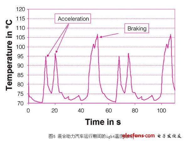
Time-varying loads must be considered for the actual thermal load of the running inverter. During the actual operation of the hybrid or electric vehicle, different load states occur: during the acceleration of the vehicle, the igbt is under a particularly high load, and during the deceleration, energy recovery is performed, and the battery of the motor is recharged, at which time the freewheeling diode is at Under maximum load. In order to describe the time-varying temperature rise of the inverter module, it is also necessary to study the behavior of the power module under a load cycle of 0.1 s to 30 s. For both configurations, the time-varying thermal resistance of igbt increases according to the width of the load pulse, as shown in Figure 4. Heat begins to flow and spread from the power semiconductor in the direction of the heat sink, causing the entire module to heat up. If the load pulse lasts longer than 30 s, the module will be heated sufficiently and the thermal resistance will no longer increase.
Time-varying thermal resistance values ​​can now be used to calculate the thermal load on the semiconductor switches and valves during operation. To do this, the actual duty cycle, as it would appear in practical applications, is used to simulate typical load conditions and load pulse widths. Let us take the hybrid vehicle drive cycle as an example, as shown in Figure 5. During the initial start-up and acceleration phases, energy comes from the battery and is sent to the motor. In these acceleration phases, the output power can reach 60kw. The temperature of igbt rises to 95 °C according to the output of the inverter. Only a small amount of inverter power is required in the constant speed phase, and the temperature of the semiconductor drops again. During the deceleration phase, the target recovers as much energy as possible and feeds it back to the battery. At this point, the power consumption of igbt and diode is about the same, while the heat dissipation is at its highest value, and the temperature of igbt reaches nearly 110 °C.
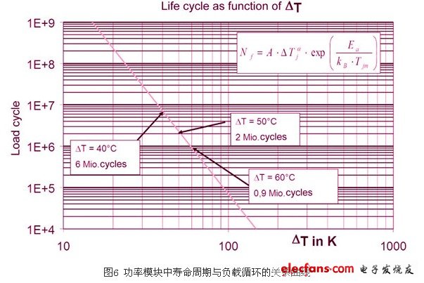
The maximum temperature rise of igbt is dt=40°C. In terms of module life, this is equivalent to 6 million load cycles, as shown in Figure 6. It can be seen that the uniform temperature distribution is important for the life and design of the inverter. If the temperature is further increased by 10 ° C - dt = 50 ° C, the number of possible load cycles will be reduced by 3 times to 2 million times. For ease of life design and optimal use of semiconductors, a uniform distribution of losses is absolutely necessary.
A uniform temperature distribution is necessary. A temperature rise of 10 °C reduces the number of load cycles by a factor of three, and a temperature rise of 20 °C can shorten the service life by a factor of six.
to sum up
The substrateless sinter module provides a range of possibilities to enhance the reliability of hybrid and electric vehicle inverter modules, and the disadvantages of soldering and expansion caused by the substrate are eliminated. The optimized layout ensures an even distribution of the temperature of the entire power semiconductor during operation. This means that the three phases can be considered equally in the calculation of the expected service life, thus facilitating the design of the inverter. The reliability of the inverter has been significantly improved, even under considerable active and passive temperature fluctuations. Many different substrateless sintering module applications have confirmed this, such as powertrains in electric vehicles and utility vehicles, as well as demanding applications such as racing cars.
10L Agriculture Drone,Spraying Drone,Uav Folding Drone,Uav Drone Crop Sprayer
Xuzhou Jitian Intelligent Equipment Co. Ltd , https://www.jitianintelligent.com