
Recently, ARM has further disclosed some of the information of ML Procesor. This article has been introduced from different perspectives and deserves our careful analysis.
Recently, ARM has further disclosed some of the information of ML Procesor. EETimes's article "Arm Gives Glimpse of AI Core"[1] and AnandTech's article "ARM Details "Project Trillium" Machine Learning Processor Architecture" were introduced from different perspectives. It is worthy of our careful analysis.
ARM disclosed that its ML Processor was on the eve of the Spring Festival this year. There was not much information released at that time, and I did a little bit of analysis (the AI ​​chip started).
This time ARM has disclosed more information and we will take a look. The first is the key Feature and some important information, and will be released in 2018.
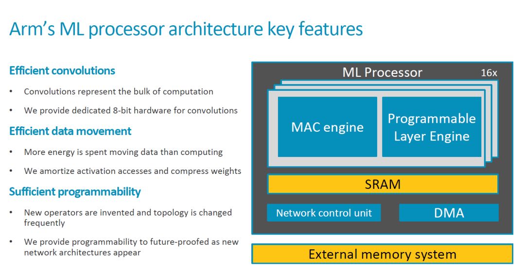
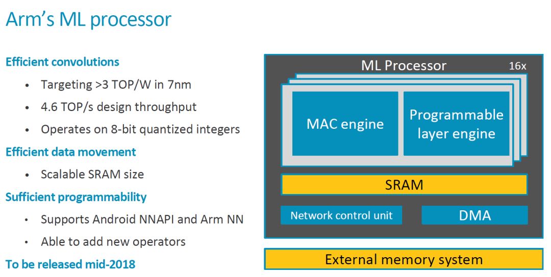
Top-level architecture
Compared with the basic block diagram initially published, we have seen a more detailed block diagram and connection relationship this time, as shown in the figure below.
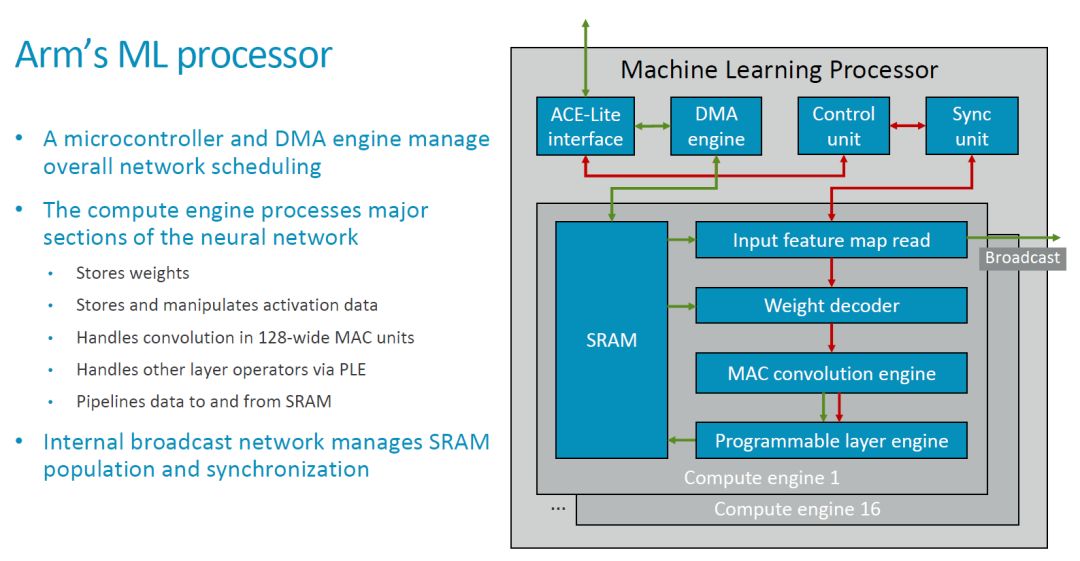
The top layer of the MLP is a typical hardware accelerator from the outside. It has local SRAM and interacts with external data and main control information (instructions) through an ACE-Lite interface. There should also be some control signals that are estimated to be omitted here (see Nvidia's NVDLA).
In the above figure, the green arrow should indicate the data flow, and the red color indicates the control flow. CE in MLP shares a set of DMA, Control Unit and Sync Unit. Its basic processing flow is as follows: 1. Configure Control Unit and DMA Engine; 2. DMA Engine reads data from the outside (such as DDR) there is local SRAM; 3. Input Feature Map Read module and Weight Read module read the feature map and weight to be calculated, processing (such as the decompression of Weight), and sent to the MAC Convolution Engine (hereinafter referred to as MCE); 4. MCE Perform operations such as convolution and transfer the result to the Programmable Layer Engine (hereafter referred to as PLE); 5. PLE performs other processing and writes the result back to the local SRAM; 6. The DMA Engine transfers the result to an external memory space (such as DDR) ).
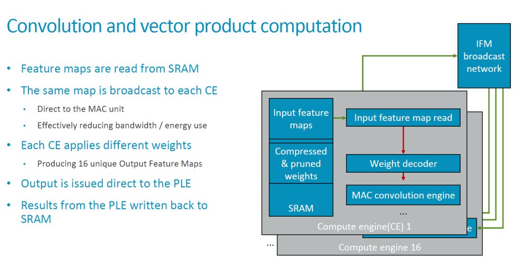
The Broadcast interface marked on the top layer implements the function of broadcasting feature map data between multiple Compute Engines (CEs for short). Therefore, the basic convolutional operation mode is that the same feature map is broadcast to multiple CEs. Different CEs use different weights to operate on these feature maps.
From the current configuration, the MLP includes 16 compute engines, each with 128 MACs, that is a total of 16x128=2048 MACs, and each cycle can perform 4096 operations. If you want to achieve the total processing power of 4.6 TOPS described by ARM, you need a clock cycle of about 1.12 GHz. Since this indicator is for the 7nm process, the problem is not significant.
MCE achieves efficient convolution
In the MLP architecture, MCE and PLE are the most important functional modules. The MCE provides the major computational capabilities (processing 90% of the computations) and should be the largest area and power consumption in the MLP. Therefore, a major goal of MCE design optimization is to achieve efficient convolution operations. Specifically, the MLP design mainly considers the following methods, most of which we have discussed before.
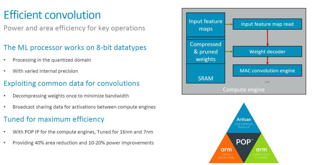
One of the more interesting points is the "varied internal precision" mentioned above. It is not yet clear what its specific meaning is. However, the application should see a fixed 8bit data type. As regards support for low-precision Inference, the information provided in [1] is, "The team is tracking research on data types down to 1-bit precision, including a novel 8-bit proposal from Microsoft. So far, the alternatives lack support In tools to make them viable, said Laudick." So in the first version of the MLP, you should not see low-precision or Bit-serial MAC anymore (see Bit-serial Processing for ISSCC 2018 in the AI ​​Chip Open Years). Introduction.)
In addition, the data compression and optimization of the process are also the main means to improve the overall efficiency. In particular, optimization of the process, combined with ARM's technology library, should have better results. This is where ARM has its advantages.
PLE achieves efficient programmability
As shown in the figure below, the structure of the PLE is basically an instruction that extends Vector processing and NN processing based on an ARM MCU. When discussing programmability, the starting point is mainly that the NN algorithm and architecture are still evolving.
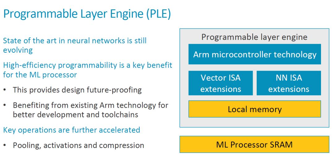
We have already analyzed the basic workflow of the entire MLP. The MCE transfers the result to the PLE after completing the operation. It can be seen from this that the MCE should send the result to the Vector Register File (VRF) and generate an interrupt to inform the CPU. After that, the CPU starts the Vector Engine to process the data. Specific as shown below.
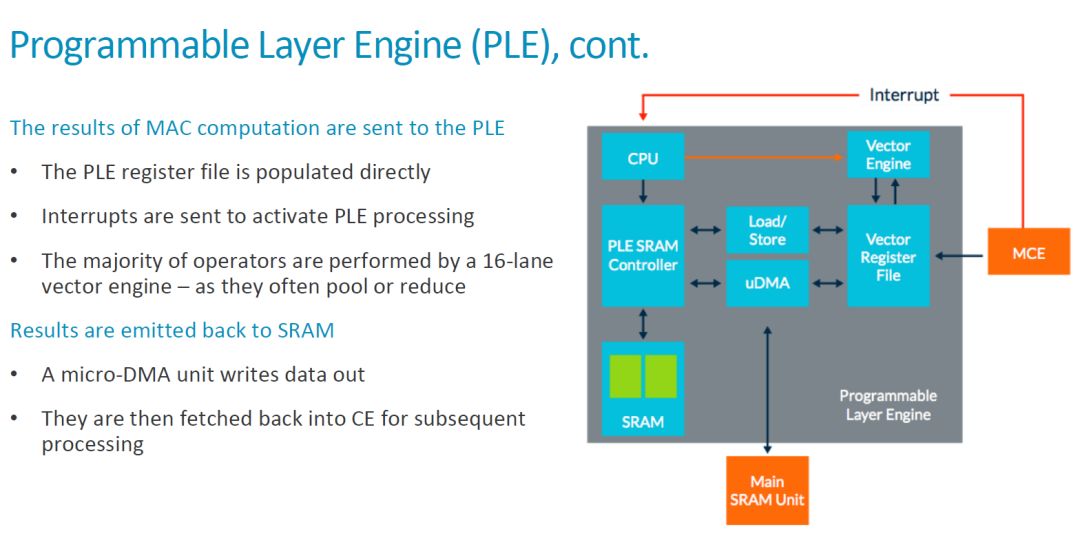
For a classmate who is a dedicated processor, the architecture of this scalar CPU+vector engine is no stranger to it. Here, there is a load/store unit and uDMA data transfer between the local SRAM, the Maing SRAM Unit (SRAM in the CE) other than VRF and PLE, and the data flow is also more flexible. Taken together, in the MLP, there is one PLE and MCE in each CE. That is, each MCE (128 MACs) corresponds to a programmable architecture. Therefore, ARM MLP's programmability and flexibility are much higher than Google TPU1 and Nvidia's NVDLA. Of course, flexibility also means more extra overhead, as stated in [1], "The programmable layer engine (PLE) on each slice of the core offers "just enough programmability to perform [neural-net] manipulations"" . High-efficient Programmability is one of the major selling points of MLP, and ARM’s “just enough†is really the most appropriate choice, and it needs further observation.
Other Information
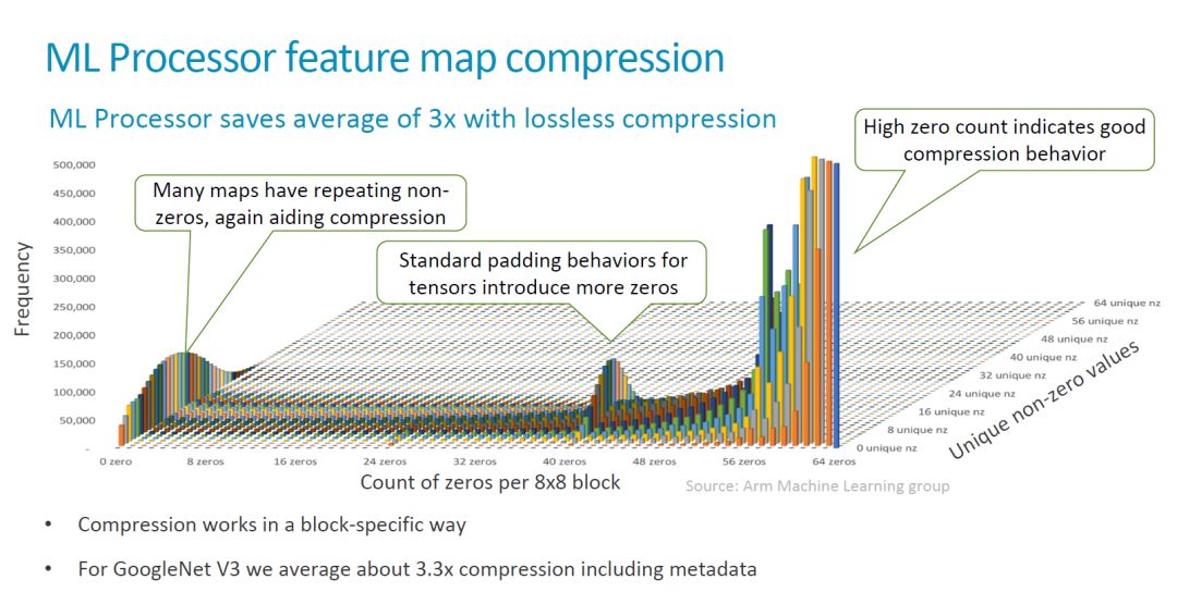
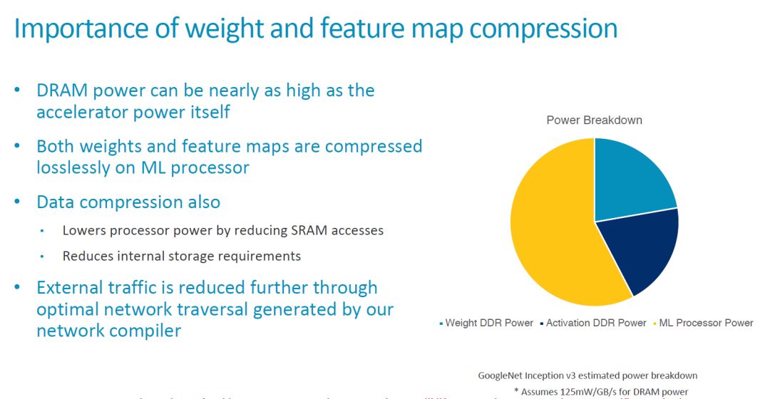
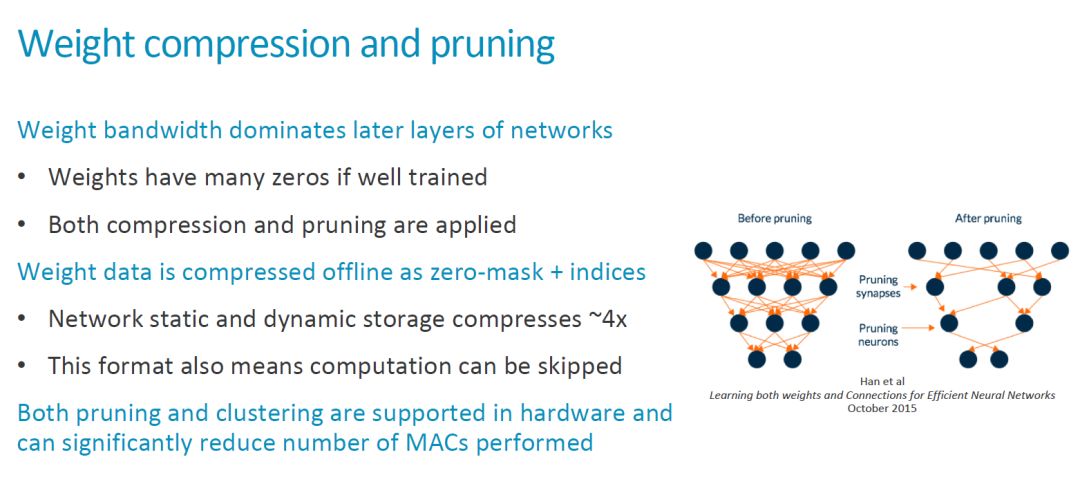
In this release, ARM also emphasized their data compression considerations, including hardware support for lossless compression. This part of the content of my previous article also has more discussion, will not repeat them, paste a few more interesting map, we see.
As an IP core, configurability is an important feature. At present, it is not known which hardware parameters of MLP can support flexible configuration. The number of Compute Engines, the number of MACs, and the size of the SRAM. These larger parameters should probably be supported for configuration. Other more detailed content depends on the final release.
In addition, the configuration of these parameters is closely related to the related software tools. More configurable parameters also mean that the software tools need corresponding support and it is more difficult. [2] In this regard, "In terms of scalability the MLP is meant to come with configurable compute engine setups from 1 CE up to 16 CEs and a scalable SRAM buffer up to 1MB. The current active designs are the 16CE and 1MB. Configurations and smaller scaled down variants will happen later on in the product lifecycle."
Competitive situation
In addition to relatively satisfactory performance indicators, ARM has not released specific areas such as MLP, power consumption, and other parameters, as well as the specific release date (currently, "production release of the RTL is on track for mid-year").
In this already "crowded" market, ARM is clearly slow. [1] Mentioned at the beginning, "Analysts generally praised the architecture as a flexible but late response to a market that is already crowded with dozens of rivals." And listed some examples of competitors.
In fact, from the perspective of ARM's key position in the processor IP market and the entire ecological chain, there is little relationship later. As stated in [1], on the one hand, ARM is working in depth with some smart phone manufacturers. "In a sign of Arm's hunger to unseat its rivals in AI, the company has "gone further than we normally would, letting [potential Smartphone customers] look under the hood"â€.
Another important advantage of ARM is that ARM has some preparations for software tools before launching MLP, including armnn and open source computing libraries, etc., as shown below.
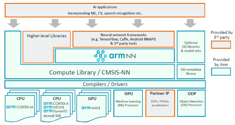
The extensive use of these tools can help ARM gain experience and optimize hardware and software tools. As quoted from ARM in [1], "Winning the hearts and minds of software developers is increasingly key in getting design wins for hardware sockets...This is kind of the start of software 2.0. For a processor company, that is Cool. But it will be a slow shift, there's a lot of things to be worked out, and the software and hardware will move in steps."
We also see that a large number of embedded AI applications are still running on various ARM hardware. Many companies have invested a great deal of effort in the optimization of related algorithms and implementations, and have also achieved good results. Of course, this brings another interesting question, that is, after the introduction of MLP in the future, where does the ML task go? How to match the different characteristics of the processor? This article just mentioned this question, "Arm will release more data on the core's performance when it is launched, probably in mid-June. But don't expect detailed guidance on when to run what AI jobs on its CPU, GPU, Or new machine-learning cores, a complex issue that the company, so far, is leaving to its SoC and OEM customers." It seems that this "hard problem" is still lost to users in the short term.
Another notable detail is that [1] mentions that "Theoretically, the design scales from 20 GOPS to 150 TOPS, but the demand for inference in the Internet of Things will pull it first to the low end. Arm is still debating. Whether it wants to design a core for the very different workloads of the data center that includes training. “We are looking at [a data center core], but it's a jump from here,†and its still early days for thoughts on a design Specific for self-driving cars, said Laudick." From here, it can be seen that at least MLP is still more scalable in processing power and should cover most of the inference applications from Edge to Cloud. If it is the highest 150TOPS, the size of the MAC should be similar to that of Google's first-generation Inference-specific TPU, but compared to Google's systolic array architecture, MLP has more complex control channels and the flexibility is much higher. Do not know the future, this will not help ARM open data center inference market.
We sell 100% original ELFBAR vape. Elf bar disposable vapes sell very well, with good taste and beautiful appearance, and are recognized by consumers. The best-selling products, such as BC5000, BC4000, BC3000, Lost Mary 5000, and new product TE5000, are sold. TSVAPE is a Chinese supplier. If you are interested, please feel free to contact us.
Disposable Pod Wholesale Rechargeable Elf Bar BC5000
The ELF BAR Disaposable Vape Kit BC5000 comes in a library of flavors, each of which is a mixture of different fruit, menthol and drinks. Because of this impeccable variety of flavor combinations, there is a little something for everyone out there.
Specification:
650mAh Built-in Battery
Rechargeable
Efficient And Consistent Power Delivery
13ml Pre-filled E-juice
5% Nicotin Level
5000 Puffs
Features:
5000 Puffs per Disposable
E-Liquid Capacity: 13ml
650mAh Battery
Dual Mesh Coils
5% (50mg) Strength Only
Type: EGO
Material: Metal
Certification: FDA, CE, ROHS, FCC
Charging Type: Wireless
Start Mode: Sensor
Disposable: Disposable
Model NO.
Elf
Nicotin Concentration
5%
Display
Without Display
Fully Charged Time


Elf Bar Vape,Fume Infinity Disposable Vape ,Disposable Vape Pen Big Smoke ,Avs Big Smoke Oem
TSVAPE Wholesale/OEM/ODM , https://www.tsecigarette.com