In the implementation of electronic converters for lighting applications, cost constraints drive the choice of technology. In addition to the innovative Vertical Smart Power (VIPower) solution described below, there are two other different classic methods on the market.
The first method is based on an IC device that, together with several external passive components, drives two high voltage (typically higher than 400V) power MOS transistors to implement a half bridge converter.
The second method is based on two high-voltage bipolar transistors and a large number of passive components, but only some of the specific functions of the other two solutions integrated as mentioned above. Bipolar solutions are used in applications where cost is extremely low and performance is low.
Compared with the classical method, this paper proposes an innovative solution, its cost is very competitive, and its performance can be enhanced.
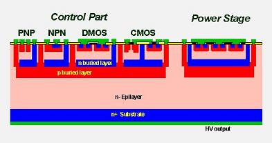
The VK06TL uses STMicroelectronics' unique Smart Power VIPower M3-3 manufacturing technology, which allows the integration of control and power stages on the same chip. The power stage is an "emitter switch" made by placing a bipolar high-voltage Darlington transistor and a low-voltage MOS field-effect transistor in a cascode structure. Therefore, this The solution achieves a balance between the low-dropout of the bipolar device and the high breakdown voltage at the off state, and the fast switching speed of the MOS field effect transistor.
Since the bipolar transistor stage is in the common base mode in the off state, the negative base current drawn from the base of the bipolar transistor is essentially the collector current, for this reason, this "emitter switch" The structure can achieve a very high frequency (around 200kHz).
This feature makes the switching performance of a cascode structure much higher than a standard bipolar crystal, comparable to a field effect MOS transistor. Therefore, we say that this device has no charge storage effect. The control part of this technology is implemented using a BCD (Bipolar-Complementary MOS-Double Diffusion MOS) cell library.
Fluorescent lamp ballast driver
Based on the VIPower M3-3 technology, we designed a driver for the fluorescent lamp ballast (VK06TL). The device is available in two different packages: the SO-16 surface mount package and the ST19 through-hole package.
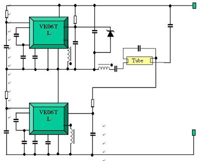
In the converter half-bridge of Figure 1, VK06TL is specified for the upper and lower arms, because with two VK06TL, almost no external components are required, and only one secondary winding can be used to turn on the primary choke Therefore, it is feasible to design a fluorescent lamp converter with extremely high efficiency and low cost.

Figure 1: M3-3 cross-section
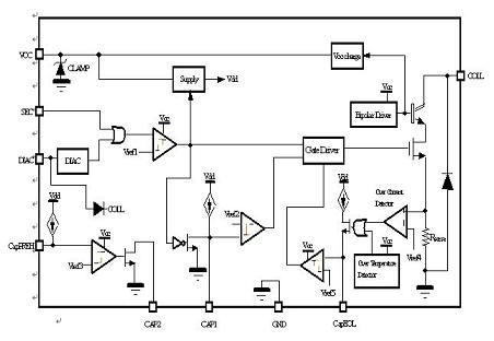
This converter properly manages all the necessary operating conditions for a high-end fluorescent lamp application: start-up, preheat frequency and duration control, ignition and steady-state phases. This half-bridge enables overcurrent protection (EOL: lamp end of life), rectification effect protection and overtemperature protection to create a fully protected system. As shown in the simplified block diagram of Figure 2: VK06TL, we consider the following factors:

Figure 2: VK06TL simplified block diagram
The power stage is a cascode-common amplifier consisting of a bipolar high-voltage Darlington transistor and a low-voltage MOS field-effect transistor. This solution achieves a low-voltage drop between a bipolar device and a high breakdown voltage at the off state. Balance, and the fast switching characteristics of MOS field effect transistors. This power stage is powered by a fixed current on the base of the bipolar transistor and is controlled by the gate terminal. In the on state (Vg > Vthreshold), the collector current can flow through the MOS transistor to the collector, and the storage phase begins.
At this stage, the emitter current no longer flows and the collector current becomes a negative base current. Because of the transmitter switch operation, the storage time is reduced to a few hundred nanoseconds (no storage effect). Once all of the base charge has been evacuated, the power stage goes into a disconnected state. Due to the short storage time, the power stage can operate at frequencies higher than the standard bipolar transistor (up to 500KHz) while maintaining a high voltage capability (up to 1KV) that cannot be achieved by standard power MOS, and conduction loss low.
Both the control and power stages are powered by the Vcc pin, which is connected to the DC bus through a resistor-capacitor (RC) network. During the startup phase, the capacitor is charged through a high-resistance resistor, so it only takes a few hundred microamps. Since the power bipolar crystal storage base current is recovered on the capacitor connected to the Vcc pin through the 'Vcc charging network', the device supplies itself to itself during the working phase.
This special feature of the VK06TL allows the use of lower power resistors, and the power supply to the bridge arm does not require a charge pump.
This device must be triggered and turned on from the SEC pin that is connected to the secondary winding. At the same time, the function of starting the oscillating circuit also requires a diode ac switching transistor. Through the SEC pin, the system can sense the resonant frequency oscillations while managing the warm-up and steady-state frequencies through the CAP1, CAP2, and CapPREH pins. In particular, the capacitor on the CapPREH pin is used to set the warm-up time.
Through the CapEOL pin, the system ensures end of lamp life (EOL) and over temperature protection. If any of these fault functions are detected, the CapEOL capacitor is charged, causing the power stage to turn off the latch. CapEOL's capacitance value is used to set the protection time.
It is worth emphasizing that this single-chip approach achieves power-level current sensing without the need for external resistors and connectors. In addition, as described above, a single temperature-protection circuit can be integrated with a single device.
Two high-voltage diodes are used for freewheeling and diode AC switching transistor channels. The typical voltage on the DC bus is 400V, because in most applications, a PFC stage (power factor controller) needs to be connected, and the collector of this device - The source breakdown voltage is guaranteed to be at a maximum of 600V.

Figure 3: VK06TL application schematic
Application board
Two reference boards have been developed: one in the SO-16 package (surface mount package) and the other in the SIP9 package (through-hole package). Both boards are based on the schematic shown in Figure 3.
Application hint
For the purpose of testing the board, it is important to connect an electrolytic capacitor (10μF, 450V) to the input terminals to bypass the parasitic inductance on the line between the DC supply voltage and the board.
The preheat frequency must be fixed to ensure that the current value is sufficient to preheat the cathode without causing the lamp to ignite.
The reference board has a preheat frequency of approximately 59 kHz and a peak current of approximately 800 mA. Since the resonant capacitor C = 8.2 nF, its voltage is lower than the preheating rated voltage (350 V peak) of a 58 W T8 lamp during the warm-up phase. The preheating time is about 0.84 s.
The steady-state phase of the main waveform on the surface-mounted package board: the operating frequency is approximately 34KHz and the peak current is approximately 700mA.
Thermal analysis of the reference board
We performed a thermal analysis of the board in Figure 3 while measuring the temperature of the device. The heat sink copper area of ​​each device is approximately 100mm2. The temperature is measured by placing a K-type thermocouple on top of the SO-16 package. The measurement environment has different external temperatures: room temperature (about 25oC) and ambient temperature (50oC). See Table 1:

Table 1: Device Case Temperature
in conclusion
This article provides an overview of ST's innovative solutions for driving linear fluorescent tubes with fixed-frequency half-bridge topologies.
The system chip method is adopted: the control part, the protection circuit and the power stage are integrated on the same chip.
System reliability has been improved by this monolithic approach. In addition, system integration and ultra-small packages have enabled smaller, less expensive application boards, a major step toward system miniaturization.
Top Plug,Top Plug In,Standard Power Conversion Plug,Power Conversion Plug
WENZHOU TENGCAI ELECTRIC CO.,LTD , https://www.tengcaielectric.com