Digital step attenuators with CMOS technology provide high ESD immunity, high linearity, low insertion loss, series and parallel logic interfaces, and a proprietary ultra low noise negative voltage generator. This article is based on Peregrine's single-chip Digital Step Attenuator (DSA) product family, which describes the DSA general design methodology, RF CMOS process, and the performance of these devices.
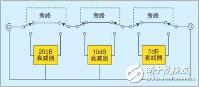
Figure 1: Typical step attenuator.
The DSA controls RF signal strength through a friendly processor interface and is used in a wide variety of RF products, such as wide dynamic range receivers, power amplifier distortion cancellation loops, and various cable distribution systems.
DSA usually has a "linear gain" characteristic and is a common interface between the ADC and the outside world. They offer higher accuracy, better temperature stability, and less distortion than analog solutions. They are also cost effective with small size, low power consumption, and ease of implementation. s solution.
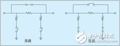
Figure 2: π-type attenuator with single-pole series switch
Although the discussion in this paper focuses on Peregrine Semiconductor's PE4302 (50Ω) and PE4304 (70Ω) 6-bit DSA devices, in fact, this DSA universal design method is applicable to all similar products.
Monolithic attenuator designFigure 1 shows a typical step attenuator with each pin of the attenuator between two single pole double throw (SPDT) switches. Mechanical relays or switches provide virtually lossless contact and are carefully designed to provide low insertion loss and excellent isolation.
For an integrated solution to deliver comparable performance, a solid-state switch with the same characteristics, low on-resistance, and a shutdown capacitor below pF is required. A FET switch operating in a linear region can basically satisfy this requirement. Although the on-resistance RON of the FET is finite, it can approach 0 Ω in a larger device. However, the cost of large devices is high, and if there is a way to reduce the number of series switches by half, such as replacing the SPDT of each unit with a single-pole single-throw switch (SPST), performance and cost can be improved.
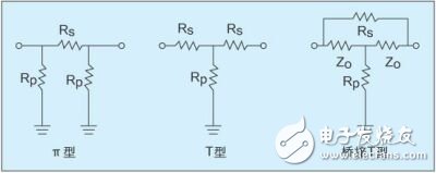
Figure 3: π-type, T-type, and bridged T-type circuits.
Figure 2 is a modified single-pole series switch structure of a π-type attenuator. In each unit, the original two SPDTs are replaced by a series SPST and two bypass SPSTs. In fact, this technique reduces the insertion loss (IL) of each cell by half, and the SPST structure is also simpler than SPDT, while performing better, especially at high frequencies.
Since all passive attenuators are three-terminal networks, this series/bypass design needs to work with other topologies, such as T-type and bridged T-type (see Figure 3). It may be because of training or customary reasons that engineers seem to prefer a π-type structure, but in a single-chip circuit with a large resistance value, this may not be the best choice.
Resistance values ​​are not an important issue when designing discrete resistors. In integrated circuits, however, the area of ​​the rectangle with a particular resistivity determines the resistance of the resistor, which is typically about 200 Ω/square in a CMOS process. The challenge for integrated circuit design is that the resistance value has become a thorny issue in the design and manufacturing process, regardless of whether the resistance is many times greater than 200 ohms or much less than 200 ohms.
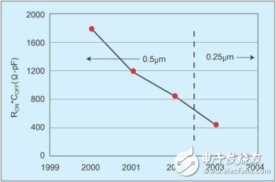
Figure 4: Development diagram of UTSi (RON/COFF) technology.
Designing very large or very small resistors requires a large area and a high cost. Large resistance resistors are long and thin square designs, while small resistance resistors have a wide profile to avoid tolerance problems. Table 1 shows the resistance values ​​of a 50Ω 6-bit binary attenuator with a least significant bit (LSB) of 0.5dB, where Rp and Rs represent the shunt resistor and series resistance in each network, respectively.
In the first row of Table 1, the step value is 0.5 dB. At this time, the resistance ratio required for the π-type and T-type networks is about 600:1 (1738/2.9 and 868/1.4), and the bridge T-type network is required. The resistance ratio is only half of it, about 300:1 (844/3). When the step value is 1dB and 2dB, the bridged T-type network still maintains a lower ratio of maximum resistance/minimum resistance value, and its resistance value range is reduced by half, at the cost of adding only one resistor.
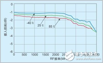
Figure 5: Typical insertion loss versus temperature.
When the step value is equal to or greater than 4 dB, the Tpp network has a higher Rpp value and becomes the best choice. This forms a general strategy: use a bridged T-type network when the step value is small, and a π-type network when the step value is large.
In either case, to make the DSA have higher accuracy, excellent linearity, minimum process error, and optimal temperature recording, the resistance of each resistor needs to be much larger than the on-resistance of the corresponding switch. . For lower dB values, the T-type structure has a higher Rp value of about a few hundred ohms, compared to the RON of the bypass switch (usually only a few ohms). Similarly, when the dB value is large, the resistance of the π-type network shunt resistor is also large, much larger than the RON of the bypass switch.
Optimization
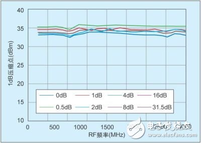
Figure 6: The 1dB compression point of the PE4302 versus frequency.
Low RON and low turn-off capacitor COFF are essential for series FET switches. A low RON means that the insertion loss is small, but it also means that a large device with a large COFF is required. However, the high-frequency working environment requires small devices with small COFF, so that the series impedance and isolation are large. This contradiction can be solved by using the largest device that provides the proper isolation. For example, when the step value is 1 dB, the isolation of the series switch is 20 dB. For an attenuating unit with a step value of 20 dB, the isolation is also a 20 dB series switch, with only 17 dB being a net change and the remaining 3 dB being an error. For this, some engineers may say: "Okay, then compensate with a higher attenuation value." Theoretically this is feasible, but in practice, the isolation is not very repetitive, COFF as long as With a little change, the isolation will vary greatly, so you must ensure that there is a suitable, rather than excessive, isolation for each step.
The voltage rating is another area that can be optimized. Each series switch must have a maximum operating voltage proportional to its attenuation value. For example, if the attenuation step is small, the incident voltage drops less. The bypass switch is completely different. Imagine the attenuator in a zero dB configuration. All attenuators are bypassed, and each bypass switch must be able to withstand the rail-to-rail input voltage.
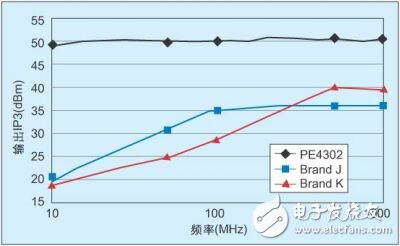
Figure 7: Comparison of IIP3 (operating voltage is 3V, insertion loss is 0dB).
Whether a series switch or a bypass switch, any one particular switch consists of one, two, three or more series FET devices. Since multiple series FETs can share the incident voltage to achieve the desired compression and intercept points, the expected voltage value determines the specific number of FET devices. As the number of series devices increases, the size of the transistors must increase synchronously to maintain the combined values ​​of RON and COFF.
In the final DSA product, the resistance is slightly higher than the value given in Table 1. Each attenuator unit adds a few tenths of a dB in its design value (insertion loss per attenuation unit) to achieve the correct net change. Finally, by placing some low-value capacitors next to the shunt resistors, the inherent high-frequency performance problems can be solved. Although this has a slight effect on the return loss, it can greatly improve the flatness and accuracy.
Install on Auto/Aircraft, Auto Signal, Recreation Vehicles, Trucks/ Trailers, Marine/ Boats,Motorbikes etc.
Be used as Direction light, emergency vehicle lamp, dashboard light, Dash light, instrument light, indicator light, stop lamp, brake light, tail Lamp, side lamp, parking lamp, tag lamp, license plate light, turn signal lamp, dome lights, interior lighting, warning indicator, etc.
Yacenter has experienced QC to check the products in each process, from developing samples to bulk, to make sure the best quality of goods. Timely communication with customers is so important during our cooperation.
If you can't find the exact product you need in the pictures,please don't go away.Just contact me freely or send your sample and drawing to us.We will reply you as soon as possible.
Brake Light Wiring,Brake Light Wiring Harness,Brake Light Harness,Christmas Light Wire Harness
Dongguan YAC Electric Co,. LTD. , https://www.yacentercns.com