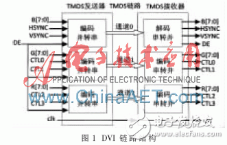
The DVI (Digital Video Interface) interface [1-3] was developed by the Digital Display Working Group in 1999 to utilize the minimum transformed differential signal TMDS as the basic electrical link signal. The three red, green, and blue signals and control signals generated by the image source are encoded and serialized by the DVI transmitter under the action of the clock, and then sent to the DVI receiver through the TMDS channel; the DVI receiver serializes/concatenates them. A series of processing such as conversion, channel alignment, and decoding are sent to the display device, as shown in FIG. The DVI interface transmits digital signals, which reduces the cost of analog-to-digital conversion, saves time and speed, and is fully compatible with HDMI in electrical features, making upgrades easier. The DVI link structure is shown in Figure 1.

DVI is received after high-speed serial long-distance transmission. The conventional method is to use receiving chip and FPGA to receive, but in the case of video signal processing with FPGA, it will undoubtedly increase system power consumption and cost. Therefore, a method for fully utilizing the FPGA's own resources to implement DVI reception is proposed, that is, an FPGA chip with built-in TMDS I/O electrical interface is used without an external dedicated chip to implement TMDS connection, and the programmability of the FPGA can make the user fast. Implement the design to shorten the design cycle.
DVI's single TMDS only provides 24-bit color depth. When the user requires a color depth of more than 24 bits, and the system has confirmed that the graphics card and display support dual-link TMDS, the system will start dual TMDS link, link 0 (data Channels 1~3) transmit 24 bit information, and other color information is transmitted by link 1 (data channel 4~6). When the user's resolution and refresh rate requirements exceed the transmission capacity of a single TMDS link (the highest pixel transmission frequency of a single link is 165 MHz), the system will initiate link 1 and define the first pixel of each line on the display. Is 1, odd pixels. Link 0 is used to transmit odd pixel information, and link 1 is used to transmit even pixel information. Since the TMDS link shares a clock loop, when the dual link works, the link clock frequency is half of the pixel data bandwidth.
The DVI encoder uses the TMDS encoding method to perform 8-bit to 10-bit and 2-bit to 10-bit encoding on the 8-bit pixel signal and the 2-bit control signal, respectively, and the least significant bit is sent first. This coding method fully embodies the two major advantages of TMDS: minimum number of transformations and DC equalization.
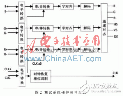
The system structure of the DVI receiver includes level conversion, clock recovery, phase adjustment, serial/parallel conversion, word alignment, channel alignment, decoding, etc. The serial signal transmitted by the TMDS channel is finally converted into 3 channels. The pixel signal of the bit and the control signal of 2 bits are as shown in FIG. 2.

Clock and synchronization are very important steps in DVI receiver design. The pixel clock provided by the DVI signal is used as the reference clock. The serial data transmitted on the TMDS channel is 10 times the reference clock, which is used when sampling at the receiving end. The rate after multiplying is sampled. In this paper, these clock signals are generated by the PLL circuit, and the data is sampled by DDR[4], which can achieve twice the serial data transmission rate. Therefore, it is only necessary to multiply the reference clock by 5 times. cost.
After the DVI signal is transmitted over a long distance, the phase uncertainty of the data and the sampling clock is large, and there is a large phase offset, which has a great influence on the correct sampling, so phase adjustment is required [5]. Using the IODELAY[4] module built into the FPGA IO interface module, the state machine dynamically adjusts the delay of the serial data to obtain the best data sampling time. Since the phase adjustment has been previously available with DCM, the IODELAY module is missing the two outputs, DCM psdone and DO[0], compared to the DCM module, thus simulating the two outputs psdone and DO[0] for the IODELAY module, Write the code in the code that calls the IODELAY module according to their timing in the DCM, completing the same function in IODELAY. Psdone is equivalent to psdone in the DCM module, indicating the completion of the first adjustment; DO[0] is equivalent to DO[0] in the DCM, indicating that the adjustment level overflows when the level exceeds 63, and the two outputs are sent to the phase adjustment. The state machine of the algorithm is used to implement dynamic adjustment. Since the video data transmitted through the TMDS channel is random, but the four control words are transmitted periodically, they can be used to detect the position of the clock relative to the data. If one of the four control words is received, the data is considered valid. As shown in Figure 3, there is a jitter region between the two sampling windows of the serial data. The jitter region describes the uncertainty of the arrival time of the clock and data on the transmission edge. The portion of the effective sampling is called a window. To ensure efficient sampling, the sampling clock must be adjusted to the center of the window.

The phase adjustment algorithm is as follows:
(1) If the initial position of the clock is at S2, increase the phase offset value of IODELAY to T1 and record it, then increase the phase offset value to T2 and record it. (T2-T1)/2 is the best. Sampling moment.
(2) If the initial position of the clock is at S1, increase the phase offset to S2, that is, start from the next jitter region, and increase the phase offset to T1 and T2 records respectively with step (1), then (T2-T1 ) /2 is the best sampling time.
Phase adjustment can also be achieved with the DCM module, eliminating the need for additional analog output signals. Unlike the phase adjustment by the DCM module, IODELAY implements phase adjustment when data is moving, while DCM is clocking. Using IODELAY can save DCM and BUFG resources in the FPGA, but an additional 200 MHz working clock is required, and the phase adjustment step and amplitude of the IODELAY module are fixed. For lower frequency DVI data, sampling window scanning may not be completed. .
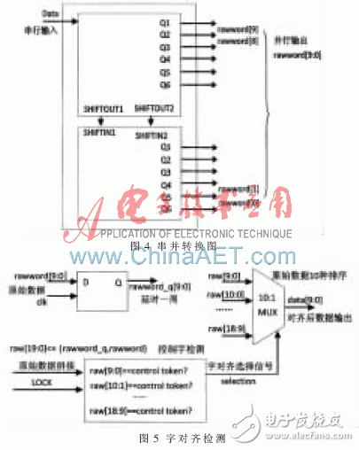
Serial/parallel conversion is accomplished using ISERDES [5] in the FPGAIO interface module, which avoids timing clutter and saves resources compared to serial/parallel conversion with a series of registers. To achieve 1:10 serial/parallel conversion, you need to concatenate two ISERDES, one is set to be the primary ISERDES, one is set to be from ISERDES, and then the output of the main ISERDES, SHIFTOUT1, SHIFTOUT2, is connected to SHIFTIN1 and SHIFTIN2 from ISERDES. ,As shown in Figure 4.

After string/parallel conversion, word alignment is also required. The BITSLIP of ISERDES itself can complete word alignment, but the speed is slower, so it is done by using multiple selector logic, as shown in Figure 5. The core idea is still to detect the control word by serial/parallel conversion of the original 10 bit data rawword[9:0] and combine it into 20 bit rawwords[19:0], and then sequentially detect rawwords[9:0] , rawwowds[10:1],...rawwords[18:9], rawwords[19:10] are equal to the control word, if they are equal, they must be rawwords[9:0], rawwowds[10:1], ...rawwords[18:9], one of rawwords[19:10], after which the data output with the correct high and low bytes can be selected by the multiplexer.
1.4 channel alignmentEach channel receives a signal from the phase adjustment state machine indicating whether the word alignment is valid. If all three channels are valid, the FIFO buffer in the channel alignment module starts transmitting data and is continuously written. And read out. The FIFO is a 16 B deep distributed RAM resource. When a channel's FIFO output detects a control word, the channel's read data stream is delayed and only resumes when the other two channels detect the control word. Channel delay can be eliminated.
1.5 DVI decodingAfter the channel alignment, the 8-bit data signal and the 2-bit control signal can be solved by the DVI decoding rule. The decoding rules are as follows: DE=0 (blanking period) solves the 2-bit control signal, and DE=1 solves the 8-bit control signal. Pixel signal.
2 simulation results This design is simulated on the modelsim6.5 version [6], and the function simulation is shown in Figure 6. Use H264E_VDATA file as Y, U, V source file, use it to generate R, G, B signals. When the transmitter reaches the receiving end, the input signal of the receiving end is the TMDS differential signals blue_p, blue_n, green_p, green_n, red_p in the figure. , red_n and clock tmdsclk_p, tmdsclk_n. The output signals are three 8-bit R, G, and B signals blue_out, green_out, red_out, and one clock recovery signal pixel_clk and control signals hsync, vsync, and de.
This design was validated on Xilinx's Virtex 5-330T FPGA. The resource utilization is shown in Table 1. Limited to the maximum output frequency of the PLL module in the FPGA is 450 MHz, so the main clock operating frequency is 90 MHz, that is, the theoretical maximum rate of TMDS serial input data is 900 Mb/s.

The actual test uses the DVI signal source output from the PC graphics card. The DVI transmission line is 1 m long, the point frequency is 74.5 MHz, and the video resolution is 1 280&TImes; 720. After the FPGA is connected to the FPGA, the DVI signal is decoded correctly. After the output parallel video data is connected to the video processing module in the FPGA, the correct dynamic video picture can be collected, and the picture is clear and noise-free, which proves the feasibility of the method.
This paper discusses a design and implementation of an FPGA-based DVI receiver that conforms to the DVI 1.0 specification. It can be verified that this method can be used for receiving and decoding DVI video, especially when using DVI decoding design by FPGA, it can reduce resource consumption, improve integration, and make full use of FPGA resources.
references
[1] Wang Chunjun, Pan Wei. The DVI Interface Should Be Embedded in Embedded System[J]. Computer Engineering, 2005, 31(20): 207-208.
[2] Yin Shuxian, Xu Huosheng. Analysis and Logic Implementation of DVI Core Technology[J].LCD & Display,2007,22(6):765-769.
[3] Feng Yongmao, Wang Ruiguang, Ding Titou. Digital Video Interface-DVI1.0[J]. Electronic Technology Application, 2003, 29(9): 10-14.
[4] Xilinx. Virtex-5 FPGA user guide[EB/OL].(2009-03-19)[2013-06-01]
[5] FENG B, CRABILL E. Video connecTIvity using TMDS I / O in Spartan-3A FPGAs [EB / OL]. (2008-07-25) [2013-06-01]
[6] Xilinx. Virtex-5 libraries guide for HDL designs [EB / OL]. (2009-09-16) [2013-06-01]
ZGAR AZ Bingo Vape
ZGAR electronic cigarette uses high-tech R&D, food grade disposable pod device and high-quality raw material. All package designs are Original IP. Our designer team is from Hong Kong. We have very high requirements for product quality, flavors taste and packaging design. The E-liquid is imported, materials are food grade, and assembly plant is medical-grade dust-free workshops.
Our products include disposable e-cigarettes, rechargeable e-cigarettes, rechargreable disposable vape pen, and various of flavors of cigarette cartridges. From 600puffs to 5000puffs, ZGAR bar Disposable offer high-tech R&D, E-cigarette improves battery capacity, We offer various of flavors and support customization. And printing designs can be customized. We have our own professional team and competitive quotations for any OEM or ODM works.
We supply OEM rechargeable disposable vape pen,OEM disposable electronic cigarette,ODM disposable vape pen,ODM disposable electronic cigarette,OEM/ODM vape pen e-cigarette,OEM/ODM atomizer device.


Disposable E-cigarette, ODM disposable electronic cigarette, vape pen atomizer , Device E-cig, OEM disposable electronic cigarette,disposable vape,zgar bingo box
ZGAR INTERNATIONAL(HK)CO., LIMITED , https://www.oemvape-pen.com