The scale of modern hardware design is gradually increasing, and the function of a single program is more and more complicated. When multiple complex programs are integrated into one FPGA, the FPGA control module is caused by the conflict of data channels and occupied resources of each program. The structure is bloated, affecting the efficiency of the entire system. The multi-configuration of the FPGA can effectively streamline the design of the control structure, while implementing a program that requires a lot of resources to implement a FPGA device with less logic resources. Based on the Virtex5 series development board and configuration memory SPI FLASH, the multiple configurations are analyzed from two aspects of hardware circuit and software design. The specific steps of multiple configuration implementation are given, which has certain reference value for implementing complex hardware design engineering.
After the FPGA completes the autoloading of the initialized bitstream at power-up, the FPGA can be reconfigured by automatically triggering a new bitstream from the address specified by the external configuration memory (SPI FLASH) by triggering multiple startup events within the FPGA. Multiple configurations of an FPGA can be implemented in a variety of ways.

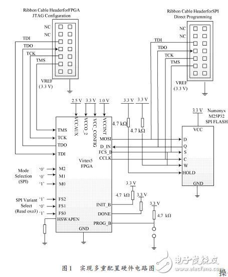
Circuit principle: The hardware of multiple configurations mainly includes the FPGA board and the FLASH chip that stores the configuration file. The FPGA uses the ML507 from the XILINX Virtex-5 family, which adds dedicated internal loading logic for FPGA multi-configuration. The FLASH chip uses XILINX's SPI FLASH chip M25P32, which has a storage space of 32 Mb. The number of storage files is related to the file size and the FPGA chip used. Implementing multiple configurations begins by connecting the FPGA and external configuration memory to the mode in which the configuration file is loaded from SPI FLASH. The block diagram of the configuration circuit hardware connection is shown in Figure 1. In the FPGA configuration mode, M2, M1, and M0 are 0, 0, 1. This configuration mode corresponds to boundary scan plus pull. In this mode, all I/Os of the FPGA are valid only during configuration. After the configuration is completed, the unused I/O will be floated. M2, M1, M0 The three selection switches correspond to the 4, 5, and 6 bits in the SW3 switch on the ML507 development board. The above switches are dialed before the FPGA is powered on. It is a 0,0,1 state.
custom cnc milling parts aluminum,cnc milling parts,cnc machining parts aluminum
Dongguan Yingxin Technology Co., Ltd. , https://www.yingxinelectronic.com