Technical requirements for CMOS integrated circuits
1. CMOS integrated circuit input requirements
The CMOS integrated circuit has a high input impedance, and its internal input terminal is connected with a diode protection circuit to prevent external interference, shock and electrostatic breakdown. When the input end of the CMOS integrated circuit is suspended, the input impedance is high, and it is susceptible to external noise interference, causing the circuit to malfunction. Destroy the normal logical relationship, and it is also very easy for the gate to induce static electricity to cause breakdown damage. Therefore, the high-level measures are taken for the redundant ends of the AND gate and the NAND gate CMOS integrated circuit; the low-level measures are taken for the redundant terminals of the OR gate or the NOT gate CMOS integrated circuit. If the operating speed of the circuit is not high, and the power consumption does not need special consideration, it can be solved by using the redundant input and the use side. The current at the input terminal should not exceed 1mA (the limit value is 10mA). The current limit must be applied to the input terminal for current limiting protection (generally, when the operating voltage is 12V, the input terminal is added with a 1.2kΩ resistor for current limiting protection). The input signal must not be greater than VDD and less than VSS, otherwise the input protection diode will cause a large current due to forward bias. When working or testing, you must first turn on the power and then add a signal, first remove the signal and then turn off the power. If the rise or fall time of the input signal is too long. It is easy to cause false triggers, which will cause the device to lose its normal function and cause loss. For the 4000B series, the rise or fall time is limited to less than 15us. Otherwise, the Schmitt trigger circuit must be used to shape the input signal. Connection to mechanical contacts at the input of a CMOS integrated circuit or application in other special cases, the input wiring is too long. The distributed capacitance and distributed inductance are large, and LC oscillation is easily formed, which destroys the protection diode in the CMOS.
The operating voltage of a CMOS integrated circuit is generally between 3 and 18 V. Since the operating voltage range of the CMOS integrated circuit is wide, a power supply circuit that does not use a regulated voltage can also operate. However, when there are gates for analog applications in the system, the minimum operating voltage should not be lower than 4.5V. Devices operating at different supply voltages will have different output impedances, operating speeds, and power dissipation. Care should be taken during use. The output of the CMOS device is not allowed to be directly connected to VCC or VSS, otherwise it will cause damage to the device.
2. Anti-static requirements
If there is no certain antistatic measures in the input circuit, CMOS integrated circuits can easily cause devastating damage to the circuit. CMOS integrated circuits should be stored and transported in antistatic materials. Workers should not wear chemical fiber clothing, hard plastic bottom shoes, hands or tools should be connected to the ground before touching the integrated block. When straightening, bending, or manually soldering the device leads, the equipment used must be well grounded. Due to the limited transient energy absorbed by the protection circuit, too large transient signals and excessive electrostatic voltages will disable the protection circuit. When soldering CMOS pins, the soldering iron must be reliably grounded, soldered with residual heat after the soldering iron is de-energized, and soldered to the grounding pin to prevent the soldering iron from leaking through the input end of the device. All in all, the static problems that may occur in the packaging, storage, transportation, welding and other aspects of CMOS integrated circuits must be treated with caution, and various measures should be taken to prevent them, and the grounding is good and reliable.
3. Interface and drive requirements
When the CMOS integrated circuit is connected to the op amp interface. The op amp uses a single power supply. And as with the power supply used by CMOS, it can be connected directly. If the op amp uses dual power supplies. CMOS uses a separate set of power supplies. In the circuit, a clamp protection circuit is used to make the CMOS input voltage between 10V and ground. The interface resistor acts both as a CMOS current limiting resistor and as a current limiting resistor for the diode. The interface circuit of the logic device should pay attention to the two problems of level matching and output capability, and should be considered in combination with the power supply voltage of the device. For example, a CMOS integrated circuit and other circuits such as TTL are connected. The power supply voltage and the input and output levels and currents of the circuits are different from each other, and the output current of the front stage circuit must satisfy the input current requirement of the latter stage circuit. The logic level of the output of the pre-stage circuit must meet the input level requirements of the latter stage circuit. The connection between them is done by level shifting or current conversion circuit. The CMOS integrated circuit can connect several similar circuits of the same chip to improve the driving capability. It is also possible to use a buffer amplifier with a strong driving capability to improve the driving capability.
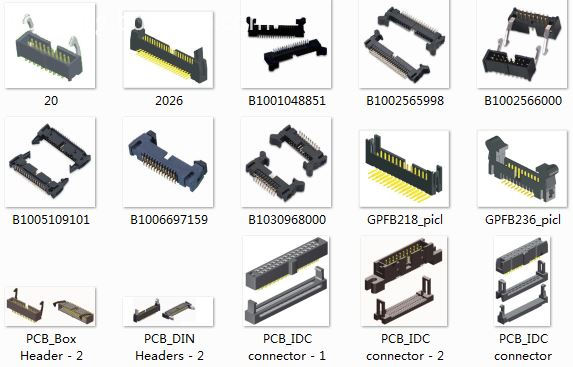
Antenk latach connector DIN 41651,Those products are used in more or less every known application within computer-, industrial-, telecommunication and specific automotive markets. This product technology allows cost effective connections between printed circuit boards based on removable or permanent connections based on a longterm proofed way of assembly. latch header connectors are available with the traditionally used pitch of 2.54mm and the pitch of 2.00mm,1.27mm.
Antenk Box Header/Ejector Header Description and Application:
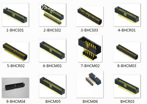
Box header/ ejector header connector, With DIP straight/vertical, SMT,Right angle, 2.54pitch, 2.0pitch, 1.27pitch,
The commonly used Pin ways have 6P,8P,10P,14P,16P,20P, 24P,26P,30P,34P, 40P,50P,64P.
Box header/ ejector header and IDC flat cable connectors are two of the most commonly used connectors. Box headers can be found in nearly all electronic equipments.
This is a IDC product which allows cost effective connections between circuit boards based on permanent connection (using transition connector) or removable connection
(Using for IDC flat cable connectors).
Box header

Ejector header

Pcb Header,Latch Header Connector,Ejector Header,Latch Ejector Connector,Box Header Connector With Latch ,Box Header Lock Type Connector
ShenZhen Antenk Electronics Co,Ltd , https://www.antenk.com