IoT applications cover a wide range of applications, including wearable devices, automobiles, residential, industrial, and even urban areas. These applications require more energy-efficient, innovative, and secure systems as support. The application is very important and aims to make software development intuitive and easy to use.
Microcontrollers (MCUs) are the core of IoT products. Choosing the right MCU is the key to satisfying customers' current and future needs. This article will explore the rich features of today's ever-increasing embedded MCUs, and MCUs can also be innovatively applied while accelerating designs. In the first part, we will introduce advanced process technology, low-power design techniques, power consumption issues of multi-core systems, multi-core communications, serial memory interfaces, and system security.
The Internet of Things market (the fastest growing engine):
Internet of Things technology constantly changes our daily work and lifestyle, making our lives more economical, convenient, comfortable and intelligent. The Internet of Things market can be broadly divided into two categories: Consumer Internet of Things and Enterprise Internet of Things.
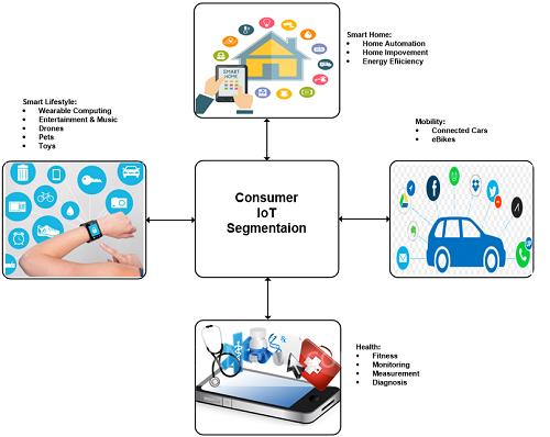
Consumer IoT includes residential, lifestyle, health, and travel. Individual users can improve their productivity, security and quality of life through these IoT device products. From smart homes to connected cars, the consumer market is preparing for the next wave.
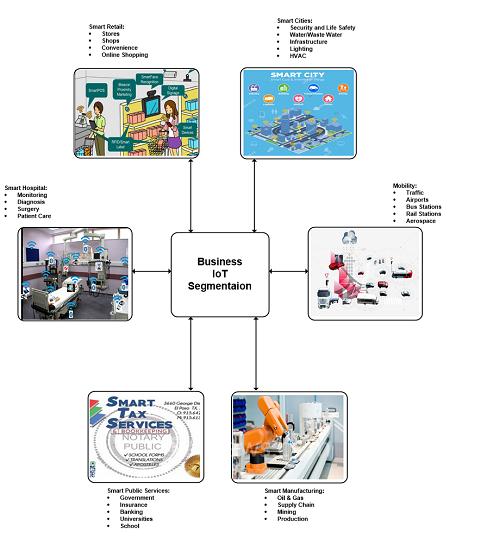
The corporate IoT has a huge coverage, including retail, medical, energy, travel, urban, manufacturing, and public services. Corporate Internet of Things segments will change organizations and communities, creating a new era for economic growth. The Internet of Things increases productivity, productivity, and day-to-day operations by connecting data, people, and machines. The corporate Internet of Things can also serve as a tool to help companies identify new growth opportunities in untapped areas.
Process Technology (Size - Very Important): Process technology for manufacturing MCUs is critical to its own performance, low power consumption, and cost. IoT applications require efficient active power consumption and low power mode consumption to improve the overall efficiency of the system. With the continuous progress in manufacturing technology, the silicon core area has been continuously reduced. More MCUs can be manufactured on the same silicon chip, which reduces the overall cost of the chip and the performance and power consumption are directly affected. The reduction in size reduces the current required to turn on/off each transistor while keeping the clock frequency constant. Therefore, a smaller chip means a higher maximum clock frequency and can achieve higher performance with lower power consumption.
For example, the 40-nanometer process technology used to manufacture Cypress Semiconductor PSoC 6 BLE series MCUs provides high-performance, energy-efficient solutions for a variety of Internet of Things applications. The current during deep sleep is only a few microamperes, and can fully retain RAM data. Other power modes, such as running, sleep, low-power operation, and low-power sleep, enable developers to flexibly optimize system power while maintaining application performance on demand.
â— Improved process technology â— Provides highly flexible power modes â— Implements power-optimized hardware IP modules â— Higher integration to reduce the number of components â— Optimize flash memory frequency â— Enable cache â— Support a wider range of operating voltage However, While process technologies have reduced size, improved performance, improved power consumption and integration, there have also been current leakage management issues, especially in low-power modes. To meet the challenge of current leakage, MCU vendors use special transistor process technologies such as multi-gate devices, high-voltage transistors/logic/circuits, specially designed memory cells, and their versatile technologies.
Flexible power modes enable developers to schedule independent system activities to optimize overall power consumption. Providing a variety of peripherals that can operate in low power modes and can be awakened to perform their functions without waking up the CPU is a key technology in this area. Some MCUs also provide peripherals that can only perform special low-power operation modes with limited functions (such as lower operating frequency and voltage) to further optimize the application power consumption, and even design specific peripherals that optimize power consumption, that is, BLE radios Designs that support low-power wireless communications can be used.
Another factor that affects power consumption is non-volatile (NV) memory access, especially MCUs that use flash memory (NV memory) to store firmware code. Any optimization of flash access will greatly reduce power consumption, and its goal is to minimize the frequency of flash memory access. Two commonly used techniques are used here, one of which is to provide a cache memory. In this way, the actual code memory (flash memory) does not need to be accessed every execution cycle. Another method is to increase the amount of data acquired in one cycle and reduce the flash memory access frequency by using a wider range of flash memory accesses.
IoT-based MCUs can also provide flexible power systems. The MCU can be powered by multiple supplies while supporting a wide range of supply voltages. For example, simple IoT applications such as fitness trackers can be powered by coin cells, and complex IoT applications such as smart watches need to be powered by PMICs (Power Management ICs). In addition, some MCUs effectively regulate their own power supply through their internal buck converters.
When considering MCU power modes, it is important to go beyond its basic architecture. For example, the standard ARM CPU core supports running, sleeping, and deep sleep. Additional power modes are usually added by specific MCU vendors. For example, Cypress's PSoC 6 BLE MCUs can perform six operating power modes, including low-power operation, low-power sleep, and hibernate.

Multi-processor MCUs (speeding up the speed of parallel application tasks): As the IoT system's functional characteristics grow, so does its complexity, and the actual size is smaller. The goal of MCU manufacturers is to improve system performance while minimizing size and reducing power consumption. Multi-core MCUs and system-on-chip (SoC) provide higher performance by integrating more functions in a single chip and minimizing chip area. A multi-core processor is an MCU or SoC that contains two or more independent cores (or CPUs). These cores are usually integrated on a single chip, they can also be used as a chip in a package.
Multi-core MCUs help provide high performance and maintain small size. Typical IoT designs, such as wearable devices, require multiple MCUs, including a BLE controller for wireless communications, a Touch MCU for executing the user interface, and a main MCU for implementing the application. The functionality of these three MCUs can be provided by a highly integrated multi-core MCU.
Multicore MCUs can bring many other benefits. For example, it can integrate enough resources to enable the CPU to handle intensive tasks in parallel, thereby maximizing the efficiency of multitasking. This also allows developers to effectively allocate system events to specific cores to achieve power and performance goals. As another example, in dual-core wearable designs, periodic functions that require less CPU intervention (such as wireless broadcast and touch sensing) can be assigned to a core. Other "frequent contact" functions, such as sensor fusion that requires frequent CPU intervention, can be assigned to another kernel. This partitioning reduces latency when multiple applications are running in the system. Integrating the protocol stack and program memory can also increase efficiency.
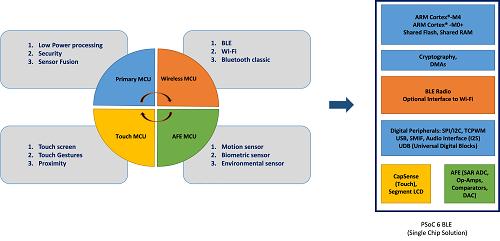
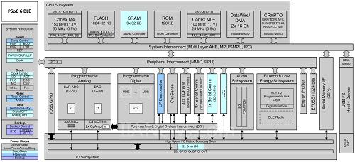
Figure 5 shows a multi-core MCU, the Cypress MCU PSoC 6 BLE. The dual-core MCU has two 32-bit ARM Cortex CPUs - Cortex-M4 and Cortex-M0+. Both CPUs are 32-bit processors with a 32-bit data path, register, and memory interface. The Cortex-M4 is a host CPU designed to achieve short interrupt response times, high code density, and high 32-bit throughput while guaranteeing tight cost and power budgets. The Cortex-M0+ acts as a secondary CPU to provide network security, physical security and protection. The Cortex CPU executes a subset of the Thumb instruction set and has two modes of operation known as thread mode and processor mode. These CPUs go into thread mode when they exit the reset and execute the application software. In order to handle abnormal conditions, the CPU enters the processor mode. When all exceptions are processed, the CPU returns to thread mode.

Interprocessor Communication (Implement Peripheral Sharing and Information Exchange):
Multicore MCUs coordinate inter-kernel operations by requiring interprocessor communications (IPC). IPC acts as a communications manager that distributes messages between processors. Modern CPU architectures (such as ARM Cortex) support multi-core communications in hardware and firmware, such as SEV (Send Event) instructions that, when executed, prompt all cores in the device. MCU vendors use a variety of methods to implement IPC:
Interrupt method: This method causes one kernel to send an interrupt to another core to indicate an application event. Usually the interrupt routine is very compact and does not take up too much code memory. As with any interrupt mechanism, each interrupt has its own ISR (interrupt service routine) through which the appropriate kernel can perform specific tasks. In the actual data transfer, there is a shared memory that can be accessed by multiple kernels. In addition to sharing data, it also provides mechanisms for requesting and acknowledging messages.
Mailboxes: Mailboxes are dedicated storage space in RAM for each CPU to send and receive messages to each other. Each kernel maintains its own RAM memory (mailbox) and sends the message to the other kernel's mailbox.
Message Queuing: Message Queuing uses two areas of shared memory to store messages that each core sends to another core. The first area is a dedicated memory called a command buffer and is used to store commands sent from the host to the slave. Another dedicated memory is called a message buffer, which enables the slave to respond to the host.
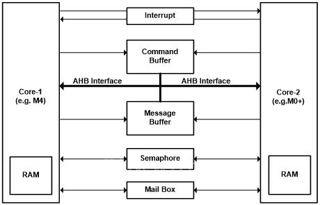
Semaphore: Semaphore is a mechanism that prevents multiple sources from accessing shared resources at the same time. In multi-core processors, the shared hardware location serves as a semaphore to indicate whether a particular kernel is using a particular shared peripheral or the like. Before accessing a peripheral, other cores in the system read the semaphore status to see if it is available.
Serial memory interface (selection of IoT memory):
Memory is an indispensable part of any Internet of Things system. Its function is mainly code and data storage. The ever-increasing intelligent demand for modern IoT devices has driven the demand for larger code and data storage. But integrating all these memories as internal memory into the device increases the chip size and cost of the MCU. Another method is to provide external expanded memory as needed. This allows developers to add memory based on the needs of the final application. In addition, if the internal storage space budget is insufficient during development, external memory can be added without having to redesign the entire system.
It is also important to understand the speed and security of the external memory interface and how to use it. In general, serial memory is better than parallel memory in saving limited IO pins on the MCU. SPI-based serial memories provide the ideal interface speed for data logging, while direct execution of external code requires higher speeds. These requirements make MCU manufacturers must provide SPI alternatives. The following is a comparison of data throughput speeds for different scenarios.
â— SPI: Supports 1-bit/cycle throughput â— Dual SPI: Supports 2-bit/cycle throughput â— Quad SPI: Supports 4-bit/cycle throughput â— Dual Quad SPI: Supports 1 byte/cycle Throughput Typically, the MCU supports multiple types of memory at the same time, giving developers maximum flexibility.
As many Internet of Things systems handle personal data of users, ensuring data security is particularly important. Code memory also needs protection to prevent equipment from being hacked. External memory is more vulnerable to security and therefore requires special mechanisms to protect externally stored data. For this reason, the MCU uses various encryption techniques (such as AES, DES, RSA) to protect data and code from illegal access. For example, Cypress Semiconductor's PSoC 6 BLE MCUs provide a special serial memory interface (SMIF) peripheral that supports XIP (live execution) mode for directly executing external code and MMIO (memory mapping) for recording data. IO) mode. It uses special commands to control, such as programming/erasing of flash memory, sleep mode input of memory devices, and so on.
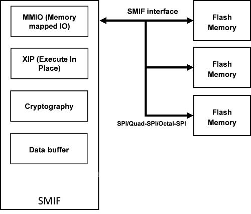
SMIF allows users to configure multiple storage devices of the same or different types and sizes. In memory (XIP) mode, multiple memory devices are mapped to different addresses. They can be different types and uses of memory, or they can be the same memory devices configured in continuous address space to simulate continuous large memory. The combination of SMIF peripherals and SPI flash memory can replace external NAND and NOR flash memory and save board space. Serial flash memory is easier to use than NAND memory because it directly maps to the processor's memory space data store and supports XIP execution.
Network security, privacy, and device security (roots of trust) of the system:
Once the device is connected to the network, there is the possibility of being hacked. Therefore, whether the device is a sports bracelet or a connected car, the security of the Internet of Things is a factor that cannot be ignored. Data protection is required at all levels, including storage, processing, and communications, to ensure system reliability. In addition, any software or firmware that handles data should be protected. This security can be achieved on two levels. The first level is software security, and the second level is hardware security, that is, hardware protection software.
Typically, security software uses keys stored in code space. Although this can technically enable encryption and decryption, this process is still vulnerable to hacking. This is because it is a stored code. When the code is decoded, security is lost.
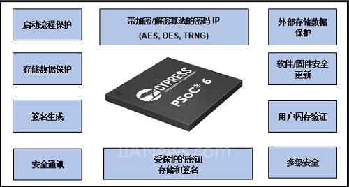
Security hardware uses integrated circuits to protect systems, such as encryption and decryption of code and data. The security hardware is independent and does not require any additional software to operate. This eliminates the possibility of malicious code, infections, contamination or other vulnerabilities from damaging the system, customer data and services. Therefore, security hardware is the preferred method when protecting sensitive data or code. So MCUs for the Internet of Things have complex integrated hardware security features such as cipher blocks, code protection IP, and other hardware-based mechanisms.
Compared with the firmware, the security hardware also has the advantage of providing faster performance and lower power consumption. For example, a dedicated encryption module in the Cypress PSoC 6 BLE MCU accelerates encryption. In addition, the module provides true random number generation functions, symmetric key encryption and decryption, hashing, message authentication, random number generation (pseudo-random and true random), cyclic redundancy check, and features such as enable/disable, interrupt settings, and Marking and other useful features. The MCU component is also equipped with a safe boot function. This function uses a ROM program to verify user data in flash memory. Secure boot is a process that incorporates encryption technology that enables IoT devices to begin executing certified, trusted software. Therefore, the system can be turned on from a known, trusted state.
In the first part, we introduced advanced process technologies, low-power design techniques, power consumption of multi-core systems, inter-kernel communication, serial memory interfaces, and system security. The second section will introduce advanced BLE wireless links, analog front ends, smart touch interfaces, and other important Internet of Things design techniques.
Get the following related material information, please click:
1. PSoC 6 BLE Family Datasheet 2. PSoC 6 BLE Architecture Technical Reference Manual (TRM)
3. PSoC 6 BLE Register Technical Reference Manual (TRM)
4. AN210781 - Getting Started with PSoC® 6 BLE 5. AN217527 - Hardware Design Considerations for PSoC® 6
MicroBT is a technology company which is based on block chain and artificial intelligence. Focusing on integrated circuit chip and products development, production and sales, and provide corresponding system solutions and technical services. We adhere the ideal"ultimate,win-win,integrity"to provide high quality products and service. Now MicroBT has passed the national high-tech enterprise certification.
As a chip design and produce company, completely design process and independent core technology. The core technology include algorithm,fine optimization of integrated circuit micro-structure ,low power technology, advanced chip packaging technology system level power and cooling technology. These core technologies and engineering methods have been successfully validated and applied in the mass production of our block chain server chips and products.
In addition to the current focus on the area of block chains, MicroBT is also responding to the national chip strategy. According to the company's development strategy and plan, MicroBT is planning to explore and extend its core R&D capabilities to other high-performance computing areas such as artificial intelligence through independent R&D and strategic cooperation.
MicroBT Whatsminer:MicroBT Whatsminer M50S,MicroBT Whatsminer M30S++,MicroBT Whatsminer M21,MicroBT Whatsminer D1,MicroBT Whatsminer M30S,MicroBT Whatsminer M10,MicroBT Whatsminer M31S+,MicroBT Whatsminer M20S
Microbt Whatsminer,M30S Microbt Whatsminer,Whatsminer Miner,M50 Miner,Asic Whatsminer
Shenzhen YLHM Technology Co., Ltd. , https://www.sggminer.com