Low-noise Amplifier (LNA) is a key component at the forefront of the receiver and is widely used in mobile communications, radar, electronic countermeasures and remote telemetry systems. Its main function is to amplify the weak signal received by the antenna from the air, reduce the noise interference, and improve the sensitivity of the received signal, so that the system can demodulate the required information data, and its noise, linearity and matching performance directly affect the whole. The performance of the receiving system, this paper focuses on the realization of the gain adjustable and improve the linearity and stability of the circuit, reduce the noise figure and improve the input / output matching characteristics of the circuit.
At present, the design of low-noise amplifiers is generally simulated by CAD. Relatively speaking, Advanced Design System (ADS) is powerful, concise and intuitive, and has a wide range of applications. This paper uses ADS software to pass linear or nonlinear operation modes. The amplifier circuit is simulated.
Receiver front end structureWhen designing the receiver, its fault tolerance should be fully considered. Once a device fails, the system can still work normally, and the redundant design method is generally used to ensure its high reliability.
As shown in Figure 1, when the LNA fails, the bypass switch can be switched so that the input signal is not directly output through the LNA, ensuring that the system can still operate normally. This design uses the PIN switch diode HSMP-4890 for bypass control. When the LNA is powered off, the signal is bypassed and alarmed by the control module. In addition, the LNA adopts a balanced structure, which ensures 50 Ω impedance matching between input and output, and is 3 dB higher than the intercept point of the single-stage amplification structure. This redundant structure also enhances the reliability of the system operation. After the loss, the LNA will still work, but the gain will be reduced by about 6 dB. The control module controls the bypass switch to turn on and off, provides power to the LNA, and adjusts the output attenuation to achieve the purpose of adjusting the gain.
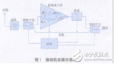
Technical specifications for LNA design: operating frequency 825 MHz - 835 MHz; noise figure "1.8 dB; gain 2 dB - 12 dB, step 1 dB; insertion loss ≤ 2.5 dB during bypass; output third-order intercept intercept point OIP3" 20 dBm; output 1 dB compression point P > 10 dBm; return loss ≥ 18 dB; maximum operating current ≤ 120 mA.
Key device selectionATF-54143 is a high gain, wide dynamic range, low noise E-PHEMT (enhanced mode pseudomorphic high electron mobility transistor), only one
Positive voltage bias, small device size, and high circuit integration make it ideal for communication systems in the 450 MHz to 6 GHz band. Moreover, according to the device performance, the highest third-order intercept point (IP3) and the lowest noise figure (NF) can be obtained when the leakage current IDS is 60 mA, and the gain is higher when the drain voltage VDS is 3 V. Simultaneously, the Xinger 1D1304-3 is a 3dB, 90 degree hybrid coupler with low insertion loss and high isolation in the 800 MHz to 1200 MHz band. It is especially suitable for balanced structure LNA designs.
Considering the adjustable gain section, the 5 bit digitally controlled attenuator HMC273 (0.7 GHz – 3.7 GHz, 1 dB – 31 dB attenuation range) can achieve a 0 dB-15 dB attenuation range by controlling the low 4 bit input high and low levels. The gain stepping requirements are met.
LNA circuit designIn general, low noise figure (NF), sufficient gain and absolute stability are mainly considered when designing LNA, but in practical applications, high intercept point, supply voltage and low current loss also need to be considered.
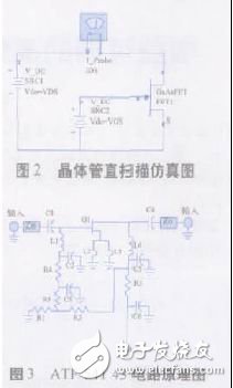
DC bias circuit designFirst, the quiescent operating point (drain current IDS and drain voltage VDS) of the device is simulated with the gate voltage VDS of the ATF-54143 as a scan parameter. Figure 2 and Figure 3 are simulation diagrams and circuit schematics, respectively. Then, according to the selected VDS (3 V), IDS (60 mA), VGS (0.56 V), the values ​​of the bias resistors are calculated by the formula (1) (2) (3).
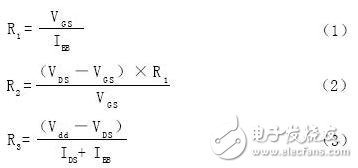
Where, IBB=2 mA is the current that flows through the R1 and R2 resistor divider networks, and Vdd=5 V is the supply voltage. The calculated bias resistor values ​​are: R1=280 Ω, R2=1220 Ω, Net R3 = 33 Ω.
Stable circuit designCircuit instability is mainly caused by three reasons: the feedback loop inside the transistor, the feedback branch generated by the external circuit outside the transistor, and the extra gain outside the passband. Absolute stability means that the circuit will not be unstable for any source and load impedance, and can usually be represented by the Rollett Stabilization Factor. The conditions for absolute stability are:

One of the improved methods is to add a small microstrip line to the ground of the transistor, which is equivalent to the negative feedback of the inductive component, which can improve the input return loss and low frequency stability, improve the linearity; A π-type resistive attenuator can be added to the output, which is also effective for improving stability.
The simulation proves that the K value will be greater than 1 in the band after the above design at the source end. However, it should be noted that the method of adding a transmission line to the source of the amplifier tube is stable at the expense of other performance of the amplifier, while an excessively long transmission line increases the possibility of self-excitation of the circuit. In order to seek balance, when the PCB is actually designed, the source microstrip line is reserved for a sufficient length. The length of the grounding can be adjusted according to the actual situation during debugging, and the excess strip line is cut off.
Matching network designInput matching networks are typically designed to achieve minimum noise, close to the optimal noise matching network rather than the optimal power matching network, while output matching networks are typically designed for maximum power and lowest standing wave ratio. Since the design requirements for LNA gain are not too high, the noise figure is first considered when designing a matching network. The input matching network is determined by the best noise reflection coefficient Topt of the component, so that the noise figure NF is minimized. According to the optimal noise figure matching condition of the S parameter simulation, the Smith chart tool provided by ADS can be very Conveniently design the input and output matching network.
It can be concluded that the input Qualcomm network L1 is 12 nH, C1 is 5.6 pF, the output high-pass matching network L4 is 15 nH, and C4 is 3 pF.
ADS simulationLinear simulation
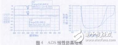
In linear analysis, the transistor can be modeled using a two-port S-parameter in Touchstone format. The hybrid coupler is modeled using a 4-port based Touchstone linear S-parameter file, which references the S2p file of ATF-54143 and the S4p of 1D1304-3. file. In order to get more realistic results, the transmission line part also uses the microstrip line model in the ADS library. In the simulation of the Spanms_wNoise of the balanced structure LNA, the length of the microstrip line is mainly adjusted to obtain the best matching result. The plate is made of polytetrafluoroethylene with a dielectric constant of 2.55, the medium thickness is 0.8 mm, and the microstrip line height is high. At 18 μm, the microstrip line width is calculated using ADS's LineCalc tool. The results of repeated trials are shown in Figure 4.
Nonlinear simulation
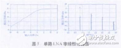
Harmonic balance (HB) simulation can be used to derive nonlinear parameters such as 1 dB compression point P and output third-order intercept point (OIP3). The main difference between the two simulation settings is the difference of the signal source. The former signal source is P_1Tone, after The P_nTone provides the tuning frequency signal, and the settings of the corresponding HB simulation are also different.
The simulation results in a P-1 dB of 16.5 dBm and an OIP3 of 32.2 dBm. The results are ideal, as shown in Figure 5.
The external input voltage is converted to 5 V using a DC-DC converter chip to provide a bias voltage to the transistor. The numerically controlled attenuator HMC273 is placed at the near end of the amplified coupling output and also requires a 5 V power supply. The 5-pin 16 dB attenuation control port is directly set high, the 1-4 pins are connected to the external input port, and the π-type resistor is placed at the far end. The circuit can be used to adjust the gain and increase the stability of the circuit. The bypass and amplifying circuit are connected at the output with a PIN switching diode HSMP-4890, which acts as an isolation to ensure low bypass insertion loss. Both the bypass and coupler input lines are 1/4 wavelength to ensure phase matching and minimize return loss.
There are a few things to keep in mind when drawing a PCB board:
(1) Calculate the width of the microstrip line according to the signal frequency and the plate parameters. In order to make up for the difference between the actual and the simulation, the impedance value is not strictly set to 50 Ω, but is higher than 1 Ω - 2 Ω. A wide range of circuit parameters can be obtained by the magnitude and location of the grounding capacitor.
(2) Reserve the adjustable capacitor position, the key is the amplifier input and output.
(3) In order to avoid interference, the RF microstrip lines and the common signal lines (control HMC273) are avoided. The middle must be separated by ground.
(4) Within the range of the line through which the RF signal passes, the underlying power line is also avoided as much as possible. The middle of the coupler can be selected to avoid changing the impedance and affecting performance.
ConclusionThe balanced structure LNA designed in this paper and the use of switching diodes to control the bypass improve the operational reliability, and the gain is adjustable in a simple and flexible way. The test results show that the actual measured LNA technical index can be well matched with the simulation results. The low noise figure of E-pHEMT tube and high OIP3 make it have great advantages in high dynamic range circuit design.
Fiber Optic Field Connector,Fiber Optic Accessory,Optical Fiber Accessories,Optical Fiber Accessory
Huizhou Fibercan Industrial Co.Ltd , https://www.fibercannetworks.com