Data converters have served as a bridge between the real world of simulation and the digital world for decades. Starting with discrete components that occupy multiple rack spaces and consume a lot of power, such as the DATRAC 11-bit 50kSPS vacuum tube ADC, which consumes 500W, the data converter has now become a highly integrated single-chip IC. Since the birth of the first commercial data converter, the endless demand for faster data rates has driven data converters to move forward. The latest incarnation of the ADC is an RF sampling ADC with a sampling rate of GHz.
Earlier ADC designs used very few digital circuits, mainly for error correction and digital drivers. A new generation of GSPS (Gigasamples per second) converters (also known as RF sampling ADCs) is implemented in cutting-edge 65 nm CMOS technology that integrates many digital processing functions to enhance ADC performance. In this way, the data converter has evolved from the large A (analog) small D (digital) ADC of the mid-1990s and early 21st century to the current small A large D-type ADC.
This does not mean that analog circuits and their performance have declined, but that the number of digital circuits has increased dramatically, complementing analog performance. These added features allow the ADC to quickly perform a large amount of digital processing in the ADC chip, sharing some of the digital processing load of the FPGA. This opens up many other possibilities for system designers. Now, with these advanced new GSPS ADCs, system designers need to design a single piece of hardware for a wide variety of platforms, and then efficiently reconfigure the hardware with software to adapt to new applications.
Enhanced high speed digital processingThe combination of shrinking CMOS process sizes and advanced design architecture means that ADCs can finally take advantage of digital processing techniques to improve performance. The breakthrough was achieved in the early 1990s, and since then, ADC designers have never looked back. As the silicon process improves (from 0.5 μm, 0.35 μm, 0.18 μm to 65 nm), the conversion speed is also improved. However, the shrinking geometry makes transistors smaller, albeit faster (and therefore higher bandwidth), but some features become slightly worse in terms of analog design performance, such as Gm (transconductance). Previously, this was compensated by adding more correction logic. However, silicon at that time was still expensive, resulting in a relatively small number of digital circuits inside the ADC. Figure 1 shows a functional block diagram of an example.
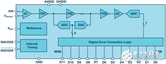
Figure 1. Early single-chip ADC with minimal digital error correction logic
As silicon technology evolves to deep sub-micron dimensions (such as 65 nm), data converters can increase the amount of digital processing in addition to the core's ability to run faster (1 GSPS or higher). This is a breakthrough that was discovered after another review. Typically, digital signal processing is handled by an ASIC or FPGA, depending on system performance and cost requirements. ASICs are dedicated circuits that require a lot of money to develop. As a result, designers often make ASIC designs work long-term to increase the return on investment in ASIC development. FPGAs are cheaper than ASICs and don't require huge development budgets. However, because FPGAs are designed to support all applications, their signal processing capabilities are limited by speed and power. This is understandable because it has the flexibility and reconfiguration capabilities that ASICs don't have. Figure 2 shows a functional block diagram of an RF sampling ADC (also known as a GSPS ADC) with a configurable digital processing block.
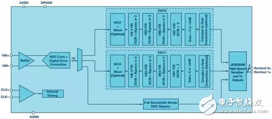
Figure 2. GSPS ADC with integrated digital processing block
The new generation of GSPS ADCs will revolutionize the radio design because it provides great flexibility in design, some of which are discussed below.
·High speed digital processingEarlier radios used a hybrid architecture of analog mixers and cascaded digital downconverters (DDCs) to downconvert the signal to baseband for processing, which involved a large amount of hardware (analog mixing) and power (analog domain and ASIC/ DDC domain in FPGA). The advent of a new generation of RF sampling ADCs allows DDCs to run at high speeds inside ADCs filled with custom digital logic, which means processing is much more efficient.
· I/O flexibility through JESD204BThe new generation RF sampling ADC not only has GSPS sampling capability, but also abandons the outdated LVDS output and uses a high-speed serial interface. The new JEDEC JESD204B specification allows digital output data to be transmitted through CML (current mode logic) at high channel rates of up to 12.5 Gbps per channel, which provides a high level of I/O flexibility. For example, an ADC can operate in full bandwidth mode and transmit digital data on multiple channels, or use one of the available DDCs and transmit the extracted/processed data on one channel as long as the output channel rate is lower than each channel 12.5 Gbps is sufficient.
· Scalable hardware designIn terms of hardware design, the use of DDC provides greater flexibility. System designers can now freeze the hardware design of the ADC and FPGA, and then make minor changes to reconfigure the system to accommodate different bandwidths as long as the ADC can support it. For example, with the provided DDC, a radio can be designed either as a full bandwidth ADC (RF sampling ADC) or as an IF sampling ADC (IF ADC). The only system change will be on the RF side, which may require very little mixing for the IF ADC. Most of the changes will be made in software, configuring the ADC to support the new bandwidth. However, the ADC + FPGA hardware design can remain essentially unchanged. This forms a benchmark hardware design that can be applied to many platforms, and the software requirements are its only variables.
More other features
The high level of integration brought by deep sub-micron CMOS technology opens up a new era in ADCs - more and more features are built into the ADC. These include fast detection of CMOS outputs that support efficient AGC (automatic gain control), as well as signal monitoring (such as peak detectors). All of these features contribute to system design, reducing external components and reducing design time.
Communication receiver design is more flexibleA very common ADC use case is the communication receiver system design. Figure 3 shows the functional block diagram of an earlier generation of radio receivers.

Figure 3. Wideband digital receiver for cellular radio
The general specifications for GSM radio receivers require an ADC with a noise spectral density (NSD) of at least 153 dBFS/Hz or better. As we all know, the SNR of NSD and ADC has the following relationship:
NSD = SNR + 10 log10 (fs ÷ 2)
among them:
The unit of SNR is dBFS
Fs = ADC sampling rate
Conventional software radio designIn broadband radio applications, simultaneous sampling and conversion of bands up to 50 MHz is not uncommon. In order to properly digitize the 50 MHz band, the ADC will require at least 5 times the sampling bandwidth, ie at least about 250 MHz. Substituting these values ​​into the above equation requires an ADC with a SNR of approximately 72 dBFS for a –153 dBFS/Hz NSD requirement.
Figure 4 shows the frequency plan used for efficient sampling of the 50 MHz band using a 250 MSPS ADC. The figure also shows the location of the second and third harmonic bands.

Figure 4. Frequency planning for a 50 MHz wideband radio with 250 MSPS ADC
The frequency of the ADC sample will fall in the first Nyquist (DC –125 MHz) band of the ADC. This phenomenon is called aliasing, so these frequencies include the target band, foldback or aliasing to the second and third harmonics of the first Nyquist band, as shown in Figure 5, as follows:
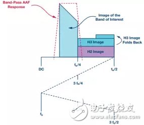
Figure 5. Available frequency bands shown in the first Nyquist zone, with secondary and third harmonics
ZGAR AZ CC Disposable
ZGAR electronic cigarette uses high-tech R&D, food grade disposable pod device and high-quality raw material. All package designs are Original IP. Our designer team is from Hong Kong. We have very high requirements for product quality, flavors taste and packaging design. The E-liquid is imported, materials are food grade, and assembly plant is medical-grade dust-free workshops.
Our products include disposable e-cigarettes, rechargeable e-cigarettes, rechargreable disposable vape pen, and various of flavors of cigarette cartridges. From 600puffs to 5000puffs, ZGAR bar Disposable offer high-tech R&D, E-cigarette improves battery capacity, We offer various of flavors and support customization. And printing designs can be customized. We have our own professional team and competitive quotations for any OEM or ODM works.
We supply OEM rechargeable disposable vape pen,OEM disposable electronic cigarette,ODM disposable vape pen,ODM disposable electronic cigarette,OEM/ODM vape pen e-cigarette,OEM/ODM atomizer device.
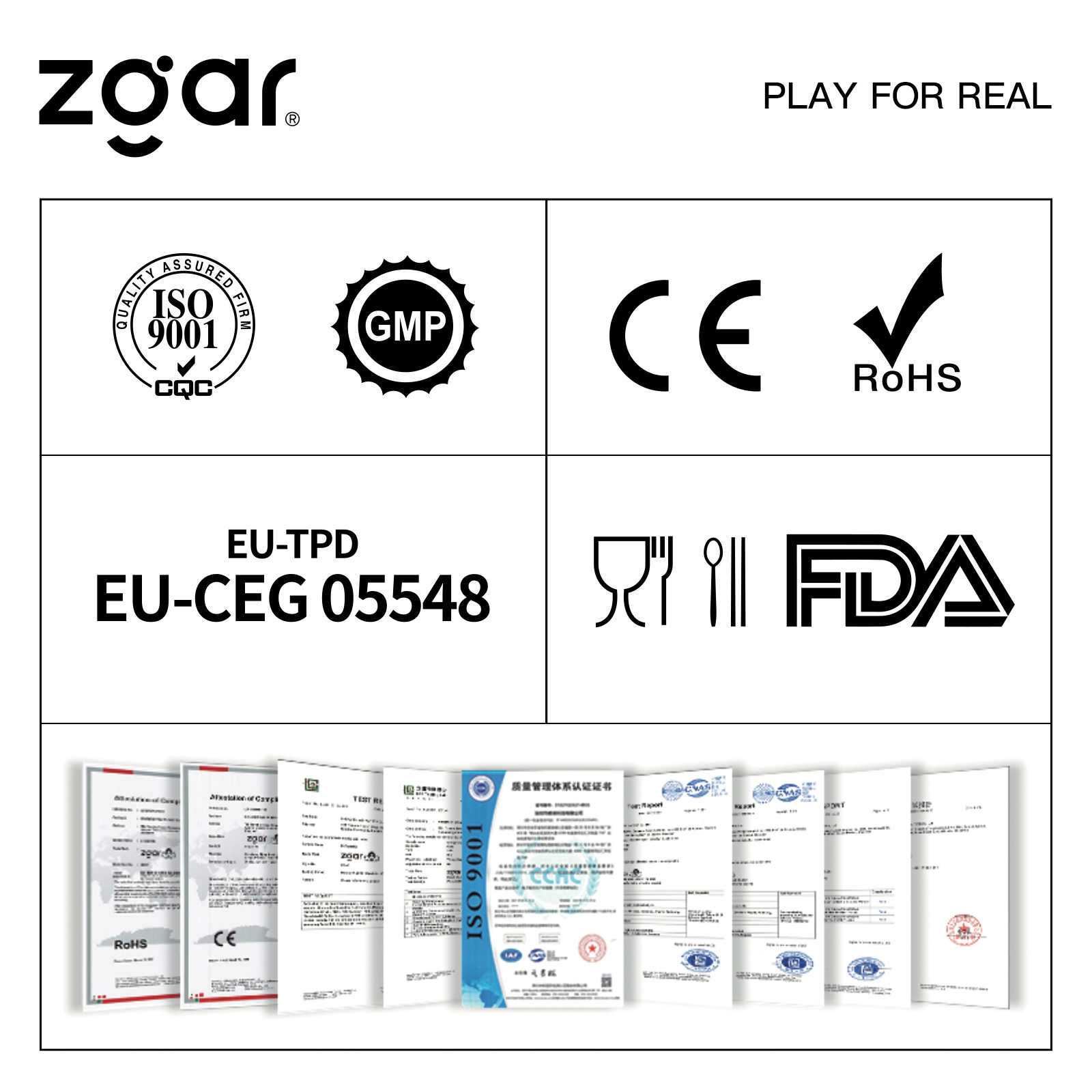
Disposable E-cigarette, ODM disposable electronic cigarette, vape pen atomizer , Device E-cig, OEM disposable electronic cigarette
ZGAR INTERNATIONAL(HK)CO., LIMITED , https://www.sze-cigarette.com