This design example describes a method for adjusting the output voltage of a power supply based on OVP/UVP testing, load margin testing, voltage programmability, or any other reason.
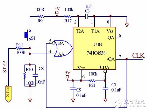
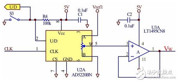
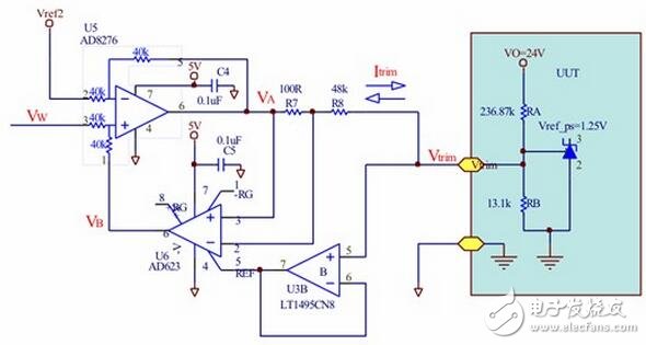
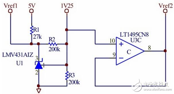
Figure 1 power supply output voltage bidirectional regulation circuit.
The circuit shown in Figure 1 can achieve bidirectional regulation of the power supply output voltage by outputting or inputting current to the feedback node. It can be operated manually via a switch or digitally via three inputs: S1 (STEP), S2 (RESET) and S3 (U/D).
Each rising edge of the S1 signal increases or decreases the output voltage VO by a step (approximately 95mV in this design). S3 controls the direction of adjustment (up/down) and S2 resets VO to the nominal value.
U4B alone ensures:
1. Add one step for each press of S1 (S1 is going to bounce).
2. There is enough time to wait for the UUT protection circuit to react.
The regulation circuit consisting of U5 and U6 features a voltage-controlled current sink/source (VCCS). U3B and U3C are used to move the VCCS reference point up to:
1. The reference point has the same level as Vref_ps and is centered. Thus, under neutral conditions (such as at reset), VW = 0.5Vref1 ≈ Vref2, Itrim≈0, VO≈VO(nominal).
2. This circuit can use a single power supply while still inputting and outputting current.
The differential amplifier U5 generates Itrim and adjusts the amplitude of the VO to reduce VO by flowing current into the Vtrim node, or sinking current to boost VO. U6 is an instrumentation amplifier with a gain equal to 1 for feeding back the detected current to U5.
The U1/U3C circuit generates two reference voltages Vref1 and Vref2. Where Vref1 is the reference voltage for the control signal Vw. Vref2 matches the UUT's 1.25V reference voltage.
Equations (1), (2), and (3) can be used to configure this circuit to obtain different VO values:
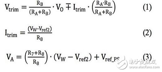
The following example inserts the parameters of Figure 1 into the above formula:
From formula (1) we can get:

Therefore, for a range of ±25% VO variation (ie 30V to 18V), Itrim ranges from -26μA to +25μA.
The range of VW is 0V to 2.5V. Substituting this value into equation (2) yields R8 ≈ 48kΩ.
According to formula (3):
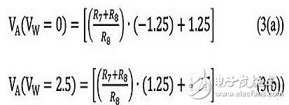
If R7=100Ω, then VA(VW=0) ≈ 0V, and VA(VW=2.5V) ≈ 2.5V
Assuming U2 has 128 steps, the resolutions of VW, Itrim, and VO are 20mV, 406nA, and 95mV, respectively.
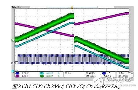
Figure 2 shows the waveforms of some key points. In the first quadrant, VO (Ch3) linearly decreases from the nominal value with each clock pulse until saturation is reached at around 18V. About halfway through, S2 is pressed, VO is reset to the nominal value, and S3 is closed. VO then rises to the upper limit of 29.5V with each clock pulse.
When the slider of U2 is in the center position, any mismatch between Vref2 and Vref_ps will cause an offset to the Itrim, causing the VO to deviate from the nominal value. Adjustment compensation can be made if needed.
The above circuit is powered by a 5V supply and consumes less than 2mA. In some applications, VO can be adjusted and used for this situation.
27 Inch Aio,All In One Pc 27 Inch,All In One Desktop Touch Screen,All In One Pc Touch Screen
Guangzhou Bolei Electronic Technology Co., Ltd. , https://www.nzpal.com