Firstly, the paper analyzes the causes and types of electromagnetic interference of switching power supply, and then deeply analyzes the design principle of EMI filter. Finally, the correctness of the theory is verified by an example.
1 Introduction Switching power supplies are characterized by high frequency, high efficiency, high power density and high reliability. However, electromagnetic interference (EMI) is very serious because its switching device operates in a high-frequency on-off state.
There are three main measures to prevent electromagnetic interference, namely shielding, filtering and grounding. Often, the use of shielding alone does not provide complete protection against electromagnetic interference. The only measure is to add a filter to cut off the path of electromagnetic interference along the signal line or power line, and together with the shielding constitute a perfect electromagnetic interference protection.
2 Switching power supply EMI generation mechanism The interference generated by the switching power supply is divided into two types according to the type of noise interference source. It can be divided into two types: peak interference and harmonic interference. If divided according to the coupling path, it can be divided into two types: conducted interference and radiated interference. . Now explain by noise interference source:
(1) Switch tube. When a large pulse current flows through the switch tube, a rectangular wave is generally formed, and the wire through which the short-circuit current generated by the waveform flows and the electromagnetic field generated by the transformer and the inductor through which the pulse current flows may form a noise source;
(2) High frequency transformer. When the originally turned on switch is turned off, the high frequency transformer generates a turn-off voltage spike, thereby forming a conducted interference;
(3) Capacitors, inductors and wires. Since the switching power supply operates at a higher frequency, the characteristics of the low-frequency components are changed, thereby generating noise;
(4) Other causes, such as interference from external input power, and the influence of the working environment of the power supply itself.
3 Conducted EMI suppression
3. 1 Conducted EMI Introduction When the harmonic level of the switching power supply is in the high frequency range (frequency range above 30MHz), it is radiated interference, and when the harmonic level of the switching power supply is in the low frequency range (frequency range 0. 15~30MHz) ) manifested as conducted interference.
Conducted interference currents can be divided into two categories according to their flow paths: one is differential mode interference current and the other is common mode interference current.
The differential mode interference and common mode interference of the switching power supply are distributed in different frequency bands:
In the cutoff frequency range, it can be divided into three frequency bands: at 0. 5MHz (also considered to be below 0.1 MHz), mainly to suppress differential mode interference; at 0. 5MHz to 1MHz (or 0.11MHz to 1MHz) In the range, differential mode and common mode interference coexist; mainly in the range of 1MHz to 30MHz to suppress common mode interference [1].
3. 2 EMI filter design theory
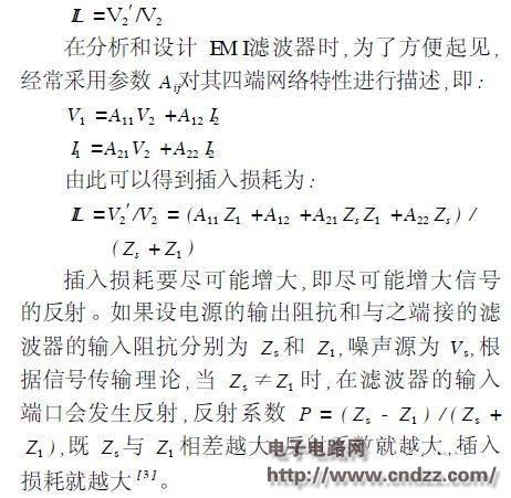
3. 2. 1 Insertion loss of EMI filter Insertion loss is one of the important technical performance parameters of the filter. The central issue to consider when designing EMI filters is to achieve the highest possible insertion loss while ensuring that the filter meets the relevant standard requirements.
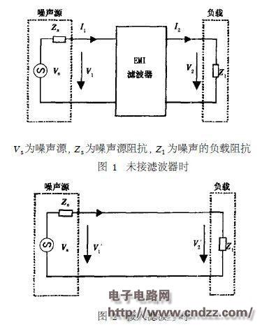
As shown in Figure 1 and Figure 2, the ratio of the output voltage before and after the access filter is the insertion loss IL:
3. 2. 2 EMI filter impedance analysis
The EMI filter is mainly used to suppress electromagnetic interference into and out of the device, and has bidirectional suppression.
From the analysis of Section 3.2.1, it is known that for the EMI filter to have the best attenuation effect on the EMI signal, the filter impedance should be mismatched with the power supply impedance, and the mismatch is more powerful, and the achieved attenuation is more ideal. The better the insertion loss characteristic.
According to the above principle, the following principles should be followed in selecting the EMI filter structure:
(1) The series inductance of the EMI filter should be connected to a low impedance source or a low impedance load;
(2) The shunt capacitor of the EMI filter should be connected to a high impedance source or a high impedance load.
3. 2. 3 Network structure of EMI filter The basic network structure of the switching power supply EMI filter is shown in Figure 3.
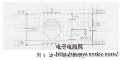
In Figure 3, the differential mode rejection capacitors are CX1 and CX2, the common mode inductor is L1, and the common mode rejection capacitors are CY1 and CY2.
The filter is composed of a low-pass filter circuit composed of an inductor and a capacitor. Since the interference signal has two modes, differential mode and common mode, the filter has an attenuation effect on both types of interference. The basic principle is:
(1) Using the characteristics of low frequency and low frequency of the capacitor, the high-frequency interference current of the positive pole of the power supply and the negative pole of the power supply is introduced into the ground (common mode), or the high-frequency interference current of the positive pole of the power supply is introduced into the negative pole of the power supply (differential mode);
(2) Using the impedance characteristics of the inductor, the high-frequency interference current is reflected back to the interference source.
3.2.4 Common mode inductance analysis
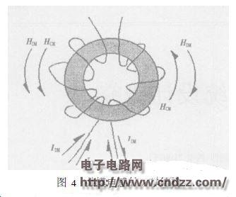
3.2.4.1 Common mode inductor working principle As shown in Figure 4, the common mode inductor is composed of two windings with opposite turns and the same number of turns on the same magnetic ring. A toroidal core is usually used, which has the characteristics of small magnetic leakage and high efficiency. When the current flows through the two windings, the resulting magnetic field is exactly offset, so that the common mode inductance does not hinder the current. If the common mode noise current passes through the common mode inductor, the common mode noise current is in the same direction. When flowing through the two windings, the generated magnetic fields are superimposed in phase, so that the common mode inductance exhibits a large inductive reactance to the interference current. This plays a role in suppressing common mode interference [2].
Actual use of the common mode inductors Two inductor windings have inductance differences due to the winding process, but this difference is just used as a differential mode inductor. Therefore, independent differential mode inductors are no longer provided in the general circuit.
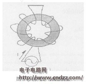
The leakage inductance measurement mode of the common mode inductor is shown in Figure 5. One end of the two windings is connected, and the inductance value is measured by the other end. The measured inductance value is the leakage inductance of the common mode inductor.
3. 2. 4. 2 Selection of common mode inductor materials To make common mode inductors, which core material should be used, in addition to the prevention of core saturation, the constant magnetic permeability of the core should also be considered. When the current is large, whether the inductance is reduced, to what extent, will it reach saturation.
Manganese-zinc ferrite, nickel-zinc ferrite and microcrystalline core are generally used in winding common mode inductors.
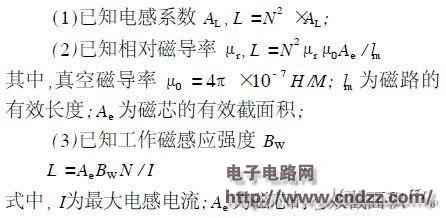
3. 2. 4. 3 Calculation of Common-Mode Inductance Value There are three methods for calculating the inductance value, which are described as follows:
4 design examples
4. 1 Filter circuit design The switching power supply parameters used in this example are: Input 24V, output 12V, power is 25W.
The filter circuit adopts a method in which the power module is added one level before and after. The common mode capacitor is 0.01μF, the differential mode capacitor is 6800pF, and the common mode inductor is made of manganese-zinc ferrite. Each pass is 31 turns and the inductance is 3.7mH.
4. 2 Filtering results When the oscilloscope bandwidth is 20MHz, the measured ripple before and after filtering is 50mV and 5mV, respectively, as shown in Figure 6 and Figure 7.
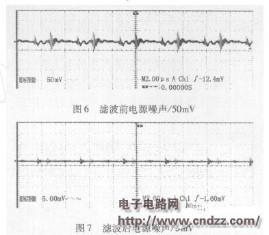
Note: The above ripples are measured under 80% pure resistive load.
4. 3 Summary Due to the complexity and particularity of EMI problems, the electromagnetic interference of different types of switching power supplies is different. It is impossible to achieve the same filtering effect for all switching power supplies by using the same EMI filter, so we have very It is necessary to master the design of the EMI filter to achieve better filtering results.
5 Conclusion Electromagnetic compatibility is a very complicated problem. When applying switching power supply, the possible electromagnetic interference problem of the power supply should be fully estimated. In this paper, the generation of switching power supply EMI is firstly described, and then the design principle of EMI filter is analyzed. Especially, the common mode inductor which plays an important role is explained in detail. Finally, under the guidance of the above theory, the design The EMI filter circuit for a certain type of switching power supply has achieved good results.
TFT LCD Arduino
TFT LCD Arduino,Active Matrix,LCD Module
Shenzhen Newvision Technology Co.Ltd , https://www.newvisionlcd.com