[performance parameters]
Available in a small LQFP64 package. 32KB of RAM, 512KB of FLASH, 16 10-bit A/D channels, and a 10-bit D/A channel.
The LPC2131 is based on a 32/16-bit ARM7TDMI-STM CPU microcontroller supporting real-time emulation and embedded tracking with 32kB, 64kB, 512 kB embedded high-speed flash memory. The 128-bit wide memory interface and unique acceleration structure allow 32-bit code to run at maximum clock rates. Applications that have tight control over code size can use the 16-bit Thumb? mode to reduce code size by more than 30% with minimal performance loss.
The small package and low power consumption make the LPC2131/2132/2138 ideal for use in small systems such as access control and POS machines. A wide range of serial communication interfaces and on-chip 8/16/32kB SRAM make the LPC2131/2132/2138 ideal for communication gateways, protocol converters, soft modems, voice recognition and low-end imaging, providing them with huge buffers Space and powerful processing capabilities. Multiple 32-bit timers, 1 or 2 10-bit 8-channel ADCs, 10-bit DACs, PWM channels, and 47 GPIOs, and up to 9 edge or level-triggered external interrupts make them ideal for industrial control and medical applications system.
characteristic
â— 16/32-bit ARM7TDMI-S microcontroller in a small LQFP64 package.
â— 8/16/32kB on-chip static RAM.
â— On-chip boot loader software is implemented in system/in-application programming (ISP/IAP). The time for sector erase or full erase is 400ms, and 1ms is programmable for 256 bytes.
â— EmbeddeDICE?RT and embedded trace interface for real-time debugging (using on-chip RealMonitor software) and high-speed trace execution code.
â— One (LPC2132/2132) or two (LPC2138) eight 10-bit A/D converters contain a total of 16 analog inputs with a conversion time of 2.44us per channel.
â— One 10-bit D/A converter with different analog outputs (LPC2132/2138).
â— 2 32-bit timer/counters (with 4 capture and 4 compare channels), PWM unit (6 outputs) and watchdog.
â— The real-time clock has an independent power supply and clock source, which greatly reduces power consumption in power-saving mode.
â— Multiple serial interfaces, including two 16C550 industry standard UARTs, two high-speed I2C interfaces (400 kbit/s), SPITM and SSP (with buffering function and variable data length).
â— Vector interrupt controller. Privilege and vector addresses can be configured.
â— Up to 47 5V general purpose I/O ports (LQFP64 package).
â— 9 edge or level triggered external interrupt pins.
â— The CPU operating frequency of up to 60MHz can be realized by the on-chip PLL, and the PLL stabilization time is 100us.
â— On-chip crystal frequency range: 1~30 MHz.
â— 2 low power modes: idle and power down.
â— Power consumption can be optimized by individually enabling/disabling external functions and lowering the external clock.
â— Wake up the processor from power-down mode with an external interrupt.
â— Single power supply with power-on reset (POR) and brownout detection (BOD) circuits:
-CPU operating voltage range: 3.0~3.6 V (3.3 V+/- 10%), the I/O port can withstand a maximum voltage of 5V.
Pin package diagram:
[Interchange compatible]
[Original (Chinese) data sheet manual foot function parameter package]

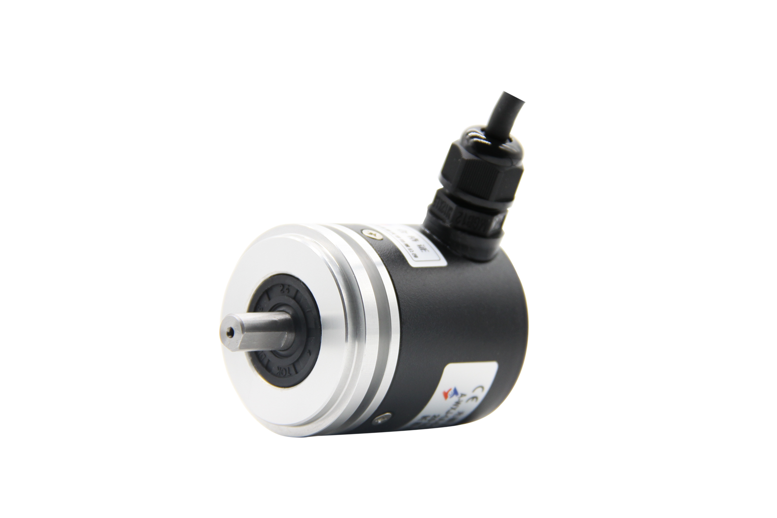
Incremental Encoder,Linear Scale Encoder,Dual Concentric Rotary Encoder,Dc Servo Motor Encoder
Yuheng Optics Co., Ltd.(Changchun) , https://www.yhencoder.com