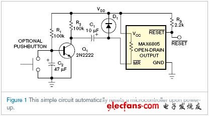
A pure manual reset is converted to an automatic reset by adding some capacitance, diodes, and resistance to the transistor and using a reset IC with adjustable hold time.
In most applications,  The (manual reset) pin is typically connected to the switch to create a manual reset signal for the management chip. Then, after a preset effective delay time, it is effectively reset from an active low to a high state. Manual reset is suitable for most applications; however, it requires human intervention to generate a reset signal. In some applications, manual reset is controversial because the system is executed each time it is powered up.
Further, applications, including embedded processors, require the reset output to remain high—that is, not active—some time before the application is reset or low-active. The circuit of Figure 1 proves to be effective when the device is powered up without pressing the reset button, because the reset automatically occurs with a preset hold time before the reset low signal arrives.

Circuit use  Pin and low active output
  Reset management chip. usually
  The internal pull-up resistor for the input is 20 to 50kΩ. During power-on,
  The internal resistor charges capacitor C1 to the positive maximum value VDD. Generated for management chip
  Reset input, its
  The input must receive an active low ground signal, requiring transistor Q1 to turn on. The length of this turn-on depends on the RC time constant of R1 and C2. These two devices determine when Q1 turns on, thus
  The output provides a high level with adjustable hold time. To increase the hold time, increase the RC of R1 and C2
The constant can be.
Reset management chip only  When the voltage of the pin exceeds the trigger threshold voltage and the internal reset period of the manager ends,
  Output. This delay time filters out the glitch of all input voltages. Because of the conduction of Q1, the negative direction of C1 becomes ground. And the positive direction of C1 cannot change the polarity immediately, it is pulled down and passed
  The internal pull-up resistor is input and slowly recharged. When the threshold voltage of the reset chip is reached, the reset signal is output once the delay time of the chip is reached. The choice of C1 is not strict. However, its value should be as large as possible - for example 0.1 to 10 μF - so that the RC time constant obtained by C1 and the internal pull-up resistor is sufficiently large. This value ensures that C1 is
  A low level of at least 1us is maintained on the pin.
After C2 is charged to the bias voltage of Q1, the transistor is still turned on. At the next power up or manual key reset circuit, transistor C2 is discharged. Once this action occurs, Q1 is turned off. R1 charges the negative direction of C1 to the supply voltage VDD. Since the forward direction of the capacitor C1 cannot be changed immediately, it appears to be charged to 2 VDD. However, protection diode D1 clamps the voltage of C1 to the VDD plus diode's turn-on voltage. The cycle is repeated once C2 is charged enough to turn Q1 back on.
Shenzhen Innovative Cloud Computer Co., Ltd. , https://www.xcypc.com