There are two modes of FPGA configuration: active configuration and passive configuration. With active configuration, we need a piece of FLASH to store the FPGA firmware, so how can we avoid FPGA upgrade failure due to unexpected situations in the process of upgrading the firmware to write FLASH What about bricks? Next, the author will lead you to dig the mountains and dig stones to find out.

This article focuses on Xilinx's Spartan-6 and 7-series FPGAs. When designing the remote upgrade function of FPGA, we have to achieve the following two indicators:
1. The FPGA has an upgrade function, that is, under normal working conditions, the FPGA can program the new firmware data into the FLASH and load it normally at the next restart;
2. If an unexpected situation occurs during the upgrade process, the original firmware in the FLASH is destroyed, then the FPGA can start the configuration from the backup firmware area, that is, there must be another firmware backup in the FLASH, and the FPGA can automatically jump to This firmware area reads the firmware.
Well, the functional requirements are clear, the next step is to concentrate on frame flow design, timing design, code writing and simulation verification. After a lot of hard work, the IP design was ready, and at this time I was secretly complacent: there should be no problem, just wait for the hardware test. Three times, five times and two times, I found a machine to test it again, and found that it can be upgraded normally. At this time, the one in my heart is happy, and it is done once, haha.
Next is an exciting brick test, so you invite colleagues around you to witness the miracle together, so the test begins, so during the upgrade operation you confidently power off, and then you face the surrounding Colleagues said: The following is the moment to witness the miracle, so you turn on the power, at this time you smile so brilliantly. Suddenly, you heard a soft, gentle whisper in your ear: man, your FPGA is brick! "How is it possible!", You snarled in disdain, but when you saw that little LED light was still asleep, you were dumbfounded, "What the hell is going on!", Look With the colleagues around me, I understand your mood: a tingling sensation of being hit hard on the face hits your heart. You buried your head and stretched your face, and tossed for a long time without finding out why, what the hell is going on?
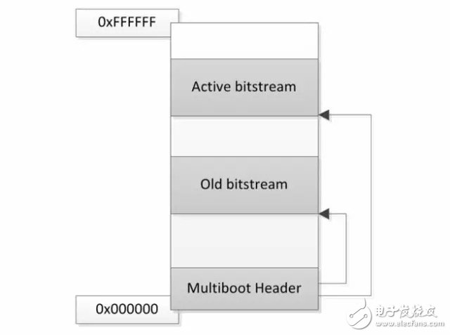
The FPGA upgrade brick also supports the FALLBACK mode, and the corresponding guidance instructions are also provided in the Xilinx official guidance document. For FALLBACK mode, the most important thing is to build a FLASH image file, the structure of the image file is shown in Figure 1.

Figure 1 FLASH image file architecture
Information about the FLASH image architecture is detailed in Xilinx ’s official configuraTIon user guide. In the figure, MulTIboot Header determines which firmware area to read the configuration file from after FPGA power-on and which firmware area to jump to to read the backup configuration if it fails. Our image is divided into two areas for storing firmware, namely: AcTIve area and Old (golden) area. Our upgrade refers to updating the firmware in the AcTIve area, and the information in the Header area and Old area is not changed; Each time the FPGA is powered on, it reads the configuration file from the Active area. The old area is a firmware backup. Its function is to enable the FPGA to start configuration from the active area when the firmware is damaged due to an unexpected upgrade.
So, how to ensure that when the firmware in the Active area is accidentally damaged due to the upgrade, the FPGA can actively switch to the Old area to read the configuration file? This is what we want to explain.
There are generally two ways to program and update FPGA firmware, as follows:
1. Sequential programming, this is the most traditional way of programming, that is, programming to FLASH without any changes to the firmware;
2. Adjust the firmware programming sequence, that is, make certain modifications to the firmware, and then program in two flashes.
The first way we thought of when designing was the first method. Moreover, the official Xilinx documentation also stated that the FPGA will jump to the backup area to start the configuration under the following conditions:
1. The synchronization word for reading the configuration file times out, and a jump will be triggered at this time;
2. If a firmware CRC error is detected, a jump will be triggered at this time.
According to these statements, there is no problem with the first method! But why not? You may find that if you test carefully, the FPGA will start from the backup area if the power is interrupted during the erasing process, and the FPGA will fail to start if the power is interrupted during the programming process. Did you see a glimmer of light? Altman said: Where there is light, there is hope! You may ask: Why is there a second way of programming? How to adjust the firmware? Why adjust? Here, I will give you a definite answer: the second method will not cause any problems. Now, we continue to sell down.
Since there are a series of questions above, then we need to study what kind of packaging format the ISE tool uses when generating firmware. After research, I found two very important information:
1. The synchronization word of the configuration file is in the first part of the firmware;
2. The CRC check command is generally at the rear of the firmware, and the FPGA must check the CRC value after receiving the CRC check command.
As mentioned earlier, the configuration jump can occur when the power-off FPGA is erased when erasing, and the configuration jump cannot be performed when the power-off FPGA is burned during programming. Speaking of this, combined with the two important findings above, you may have Have you found the answer to your own question? Obviously, because there are few synchronization words in the firmware, they can be erased quickly and can be written into FLASH quickly; therefore, when the power is turned off during erasing, the synchronization words of the firmware have been destroyed, and the FPGA read The watchdog timeout will occur if the synchronization word is not reached, then the FPGA will jump to the backup area to read the configuration file; when the power is turned off during programming? Because the synchronization word has been correctly written at this time, and the CRC check command is destroyed, the FPGA will read the CRC check command during configuration until it is read, but what if the CRC check command is damaged? There is no way, FPGA has a toughness and perseverance that does not hit the south wall and does not look back. If it hits the south wall, it still does not look back. It will keep reading, so it will fall into an endless loop, hey! You said how great it would be if you had this spirit in love too!
After the above explanation, we will suddenly realize: It turns out that the FPGA configuration jump triggered by the CRC error is not reliable! In this case, we can only write on the synchronization word of the firmware. Well, do n’t sell it, in fact, writing on the synchronization word of the firmware corresponds to the way of upgrading the firmware 2: Modify the firmware and adjust the order of the firmware. The simple explanation is as follows:
1. Modify the synchronization word of the firmware, and do not burn the synchronization word during the first programming step;
2. When the rest of the firmware is burned, the synchronization word of the firmware will be burned into the corresponding FLASH position.

After doing so, whether the power is lost during the erasing process or the process of programming, the synchronization word of the firmware will be destroyed. Then the configuration jump of the FPGA will be triggered, that is, FALLBACK will succeed! A little spoiler: the AR Q & A record on the Xilinx official website also has a corresponding solution description, go search it yourself, and good luck!
The 8-inch tablet will have a big impact on the 7-inch and 10-inch tablet market. Because the portability of an 8-inch tablet is stronger than that of a 10-inch tablet, and the usable area is larger than that of a 7-inch tablet. The most important thing is that the price is more moderate, which is much cheaper than a 10-inch tablet. It can be said that the 8-inch tablet computer has a good balance between portability and screen display area, and is more likely to be favored by the majority of users.
8 Inches Tablet Pc,Tablet Computer,8 Inch Android Tablets,8 Inch Tablet
Jingjiang Gisen Technology Co.,Ltd , https://www.gisentech.com