A sine wave inverter, we first think of SPWM technology. How to achieve SPWM? Certainly many people's first idea is to use a single-chip. Indeed, the benefits of using a single-chip microcomputer are many: SPWM wave high precision, output sine wave waveform is good, High voltage regulation accuracy, easy to add voltage indication function, etc., MCU is very suitable for industrial mass production. But for our players, this is not the case. MCU is not everyone can master, even if mastered, like me, only do electronic clock It is also difficult for junior players such as infrared remote control to write good SPWM programs. Therefore, I considered the full hardware solution.
The advantages of this circuit:
1. The circuit is extremely simple, probably the world's simplest discrete SPWM circuit
2. Single power supply wide voltage supply (10V-30V)
3. The output maximum duty ratio is high. The maximum duty cycle is close to 100% during simulation. This will result in high bus voltage utilization, and the bus voltage 340V is enough to generate 230V power frequency sinusoidal AC.
4. Isolated output, less interference from peripheral circuits After a few days of thinking, I determined the block diagram of the system: 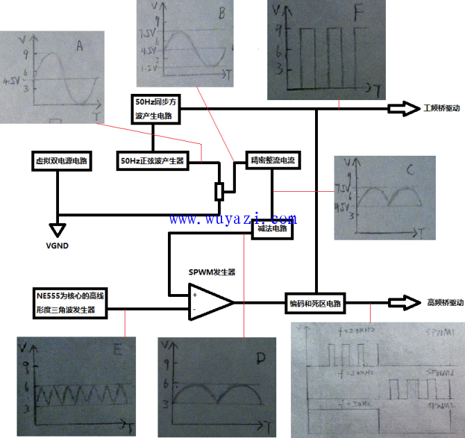
This circuit does not use the voltage feedback, so the voltage regulation function is completed by the front stage. The front stage is generally composed of SG3525 or TL494, and the voltage regulation function is not a pity.
Look at this picture, because the virtual dual power supply is used, a single power supply can be used, omitting an auxiliary power transformer.
Look at the driver board circuit diagram: 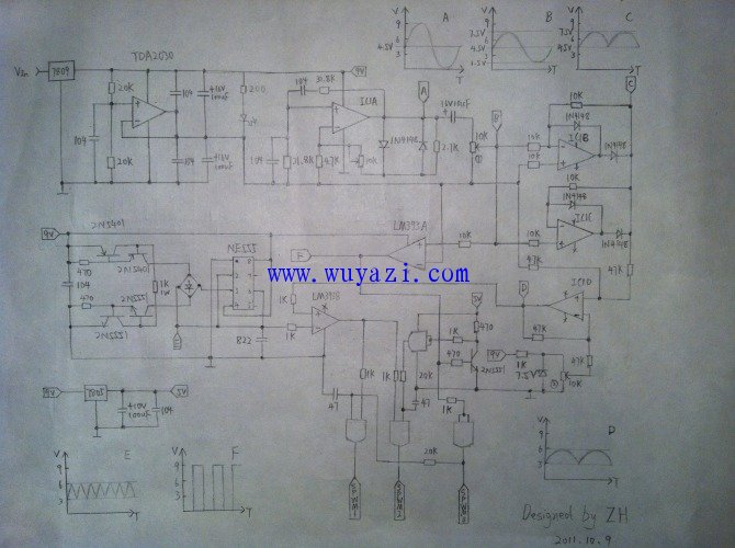
The sparrow is small and complete. As shown in the figure, the LM7809 reduces the battery voltage to a stable 9V, which allows the circuit to operate in a wide power supply (10V-30V). The TDA2030 is a core dual virtual power supply that turns positive 9V into a The dual-supply with positive and negative 4.5V. NE555 and peripheral components form a high-linearity triangular wave oscillator with a frequency of about 20KHz. As shown in the figure, the triangular wave that moves between 3V and 6V can be obtained at the 2 and 6 feet of NE555. IC1 is LM324. IC1A and peripheral components form a 50Hz power frequency sinusoidal oscillator, which produces a sine wave with a amplitude of 4.5V (for the virtual ground generated). The potentiometer divides the amplitude of this sine wave to 3.5V. IC1B and IC1C and peripheral components The precision rectification circuit converts the sine wave into a 3V-valued taro wave. This taro wave is going to be compared with the triangular wave of the NE555. Although the amplitudes of the triangular wave and the taro wave are the same, both are 3V, but the lowest potential of the taro wave is triangular. The height is 1.5V. Therefore, IC1D and peripheral components form a subtraction circuit, which reduces the overall value of the skull wave by 1.5V, so that the triangular wave and the skull wave can be compared. The LM393B performs comparison work to generate the same phase SPWM wave, which is composed of LM393A. Sine wave-square wave converter The synchronous square wave is sent into the encoding circuit composed of CD4081 and encoded to generate the SPWM signal of the final driving power tube. Two 20K resistors and 47P capacitors are used to generate the dead zone on the high frequency arm. One of the clever places in this circuit design is Virtual land and field conversion. The circuit before LM393A is working in the virtual ground state, and the circuit after LM393 has become the ground. Because 4.5V AC (for virtual ground) is a 9V pulse for the field. LM393B periphery The circuit is similar to the principle.
Then look at the H-bridge circuit diagram: 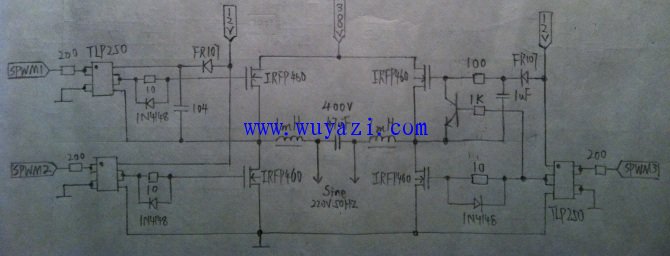
The above is the H-bridge circuit. Note: The grounding symbol on the side of the three TLP250 must be connected to the ground of the driver board! The ground of the power tube can also be shared with the front stage (connected to the battery). It can also be isolated from the front and rear stages. The 12V voltage can be supplied by the main transformer's sub-winding + LM7812 (front and rear stage isolation scheme), or it can be directly provided by the battery (in the case of 12V power supply, the front and rear stages are not isolated, the common ground state).
First analyze the left high frequency arm: the IRFP460 of the lower arm is directly driven by the diaphragm, and the IRFP460 of the upper arm is driven by the bootstrap capacitor + diaphragm. The working principle is short: when the lower arm is turned on, the midpoint of the power tube of the high frequency bridge Equivalent to grounding. At this time, the bootstrap capacitor of 104 is charged by the FR107 and the lower arm. When the lower arm is turned off, the 104 capacitor is isolated from the ground. When the internal transistor of the TLP250 is turned on, it is equivalent to the GS of the upper arm. A voltage is applied between them, so the upper arm can be turned on and off under the control of the corresponding TLP250.
Then analyze the power frequency arm on the right side: this part of the circuit uses a half bridge in my one. When the TLP250 outputs a high level, the lower arm of the power frequency bridge is turned on, and the midpoint of the power frequency bridge is equivalently grounded. The 1uF capacitor is charged by the FR107 and the lower arm tube. However, since the triode is also turned on, the upper arm tube has a relative voltage between GS at this time, so the upper arm tube is turned off. When the TLP250 outputs a low level, the lower arm tube and the triode are closed. The turn-off of the triode and the voltage stored on the capacitor cause the upper arm to conduct. The power frequency arm works like this, so either the upper tube is conducting or the lower tube is conducting. Since the SPWM3 is a 50 Hz pulse, it can be used. The midpoint of the bridge is 50Hz, 50% duty cycle AC voltage.
Two 1mH inductors and one 400V 40uF capacitor are used to perform the task of high frequency filtering, turning the high frequency SPWM square wave into a 50Hz sine wave.
The principle analysis is completed.
Finally, let me talk about how to debug:
Assembly circuit
2. Look at the waveform of point A, which should be a sine wave with a 50Hz amplitude of 4.5V (for virtual ground)
3. Adjust the potentiometer of the circle 1 so that the sliding end (B) has a sine wave pulse of 3V amplitude (to the virtual ground) on the virtual ground. At this point, the head wave of the amplitude 3V frequency 100Hz can be seen at point C (for the virtual Ground)
4. Adjust the potentiometer of the circle 2, which has a voltage of 1.5V from the sliding end to the ground (in the ground). At this point, the head wave with the amplitude of 3V and the upward offset of 3V in the ground can be seen at point D.
5. Test the E point, you can see a triangle wave with a frequency of 3V amplitude of 3VHz, which is offset by 3V amplitude, and a 50Hz pulse square wave with a magnitude of 9V.
6. At the output of the LM393B, an SPWM pulse with an amplitude of 9V should be measurable.
7. Test the waveform of SPWM1-3, as shown in the figure: 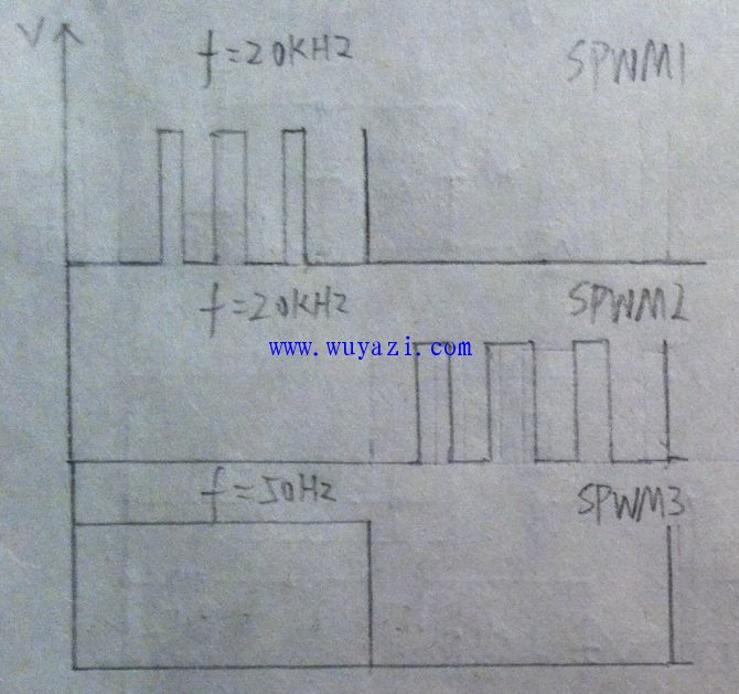
Finally, I wish the success of the trial comrades! This circuit is completely based on simulation, and may cause minor problems in actual production. Welcome everyone to correct criticism!
The waveform of the sub-simulation: 
08*16 2835 Led Neon Flex,Neon Flexible,Neon Flex Light,Neon Flex Led Strip
NINGBO SENTU ART AND CRAFT CO.,LTD. , https://www.lightworld-sentu.com