The circuit board is the carrier of electronic design. It is the place where all electronic components and circuits are summarized. Nowadays, there are more and more electronic products, more and more components, more and more complicated circuit design, and the most basic single. The panel can no longer be used universally. When the single-sided circuit is insufficient to provide the electronic component connection requirements, the circuit can be arranged on both sides of the substrate, and a through-hole circuit is arranged on the board to connect the circuits on both sides of the board. This type of PCB is called a double-layer pcb board.
Double-layer PCB board manufacturing process and processThe two-layer PCB production process can be roughly divided into the following parts:
Printed circuit board - inner layer - press-drill - plated through hole (primary copper) - outer layer (secondary copper) - anti-weld green paint - text printing - joint processing - forming cutting - final inspection packaging.
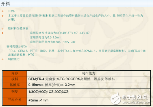
1. After processing the customer's original data of the PCB, after confirming that there is no problem and conforming to the process capability, the first station entered will determine the PCB substrate size, PCB material and number of layers according to the work order issued by the engineer. ...etc. to send out the material, in simple terms, is the material needed to prepare the PCB.
2. Inner film dry film dry film (Dry Film): It is a resisting agent capable of sensitizing, developing, anti-plating and anti-etching. The photoresist is attached to the cleaned surface by hot pressing. The water-soluble dry film is mainly due to the organic acid salt in its composition, which reacts with a strong base to form a salt of an organic acid, which can be dissolved by water. It is composed of a water-soluble dry film, which is imaged by sodium carbonate and stripped with dilute sodium hydroxide. The imaging action done by the film. This step will “stick†the surface of the finished PCB to a water-soluble dry film that will undergo photochemical reaction, which can be sensitized to represent all the lines on the PCB.
3. After exposing the copper plate after lamination, the negative film is automatically positioned by the computer and then exposed, so that the dry film of the plate surface is hardened by photochemical reaction, so as to facilitate subsequent copper etching. Exposure intensity and exposure time
4. The inner layer development will remove the exposed dry film by the uncoated dry film.
5. Acidic etching etches the exposed copper to obtain the PCB trace.
6. To dry the film, this step is then washed with the syrup to adhere to the hardened dry film on the surface of the copper plate. The entire PCB circuit layer has been roughly formed.
7. AOI uses the automatic optical alignment inspection machine to check the alignment of the correct PCB data to detect whether there is an open circuit, etc. If this is the case, it will be repaired for the PCB.
8. Blackening This step is to treat the copper on the surface of the PCB with the correct water after the inspection, so that the copper surface is fluffy and increase the surface area to facilitate the bonding of the two sides of the PCB layer.
9. Pressing and pressing the machine with hot pressing, press the steel plate on the PCB, after a certain time, after reaching the required thickness and determining the complete bonding, the bonding work of the two sides of the PCB layer is completed.
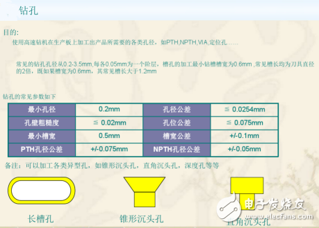
10. After drilling the engineering data into the computer, it is automatically positioned by the computer, and the drills of different sizes are exchanged for drilling. Since the entire PCB has been packaged, an X-RAY scan is required to find the hole necessary for the drilling procedure after the positioning hole is drilled.
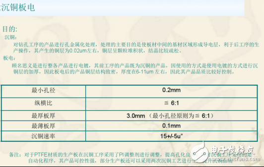
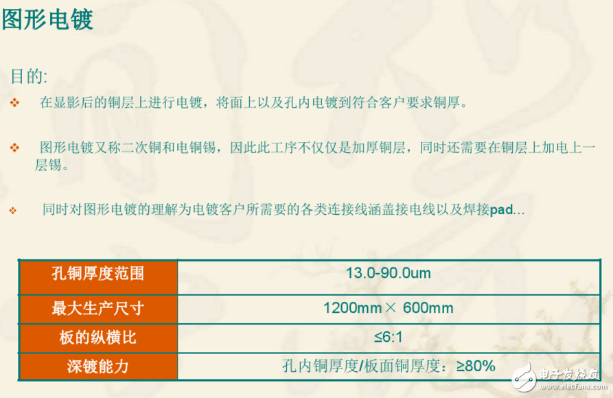
11.PTH Since the layers in the PCB are not turned on, it is necessary to plate copper on the drilled holes for interlayer conduction, but the Resin between the layers is not conducive to copper plating, and it is necessary to make a thin layer on the surface. The chemical copper is then reacted with copper to achieve the functional needs of the PCB.
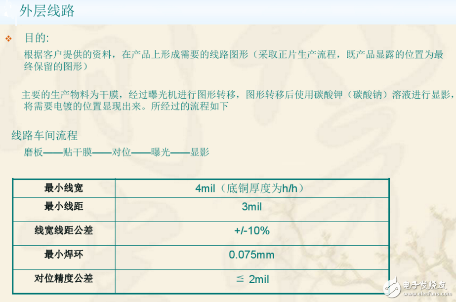
12. External lamination film pre-treatment After drilling and through-hole plating, the inner and outer layers are connected, and then the outer layer is fabricated to complete the circuit board. The lamination is the same as the previous lamination step in order to make the outer layer of the PCB.
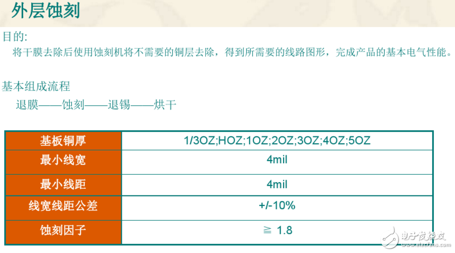
13. Outer layer exposure with previous exposure steps
14. Outer layer development and previous development steps
15. Line etching outer circuit is formed in this process
16. Remove the dry film to dry film. This step is followed by washing with the syrup to adhere to the hardened dry film on the surface of the copper plate. The entire PCB circuit layer has been roughly formed.
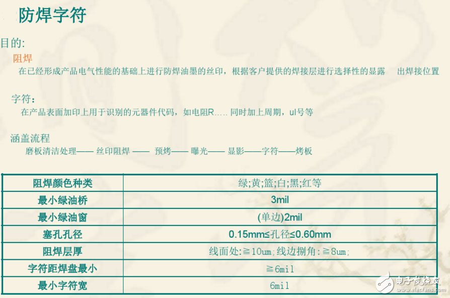
17. Spraying Apply the appropriate concentration of green paint evenly on the PCB, or evenly spread the ink on the PCB by using a doctor blade and a screen.
18.S/M uses light to harden the part that needs to retain green paint. The part that is not exposed to light will be washed away in the development process.
19. The image is washed with water to remove the unhardened portion, leaving a portion that hardens and cannot be washed away. Bake the dried green paint and make sure it is firmly attached to the PCB.
20. Printed text printed on the appropriate stencil according to customer requirements, such as the item number, date of manufacture, location of the part, manufacturer and customer name.
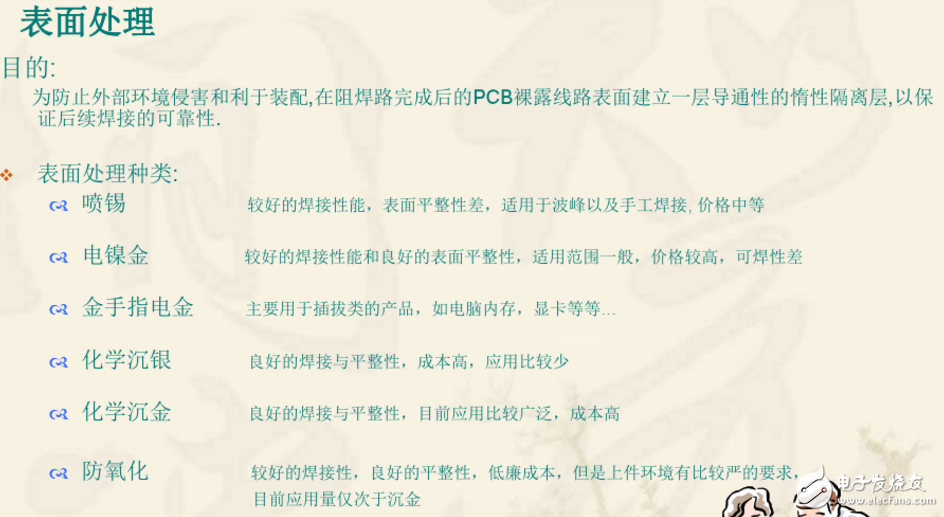
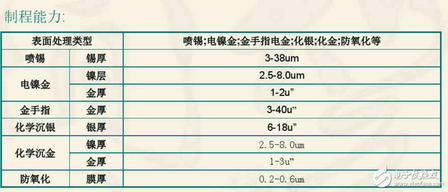
21. In order to prevent the bare copper surface of the PCB from being oxidized and to maintain good solderability, the board factory needs to surface-treat the PCB, such as HASL, OSP, chemical immersion silver, nickel immersion gold...
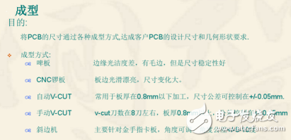
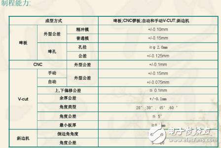
22. Molding CNC milling cutter cuts the PCB of the large Panel into the size required by the customer.
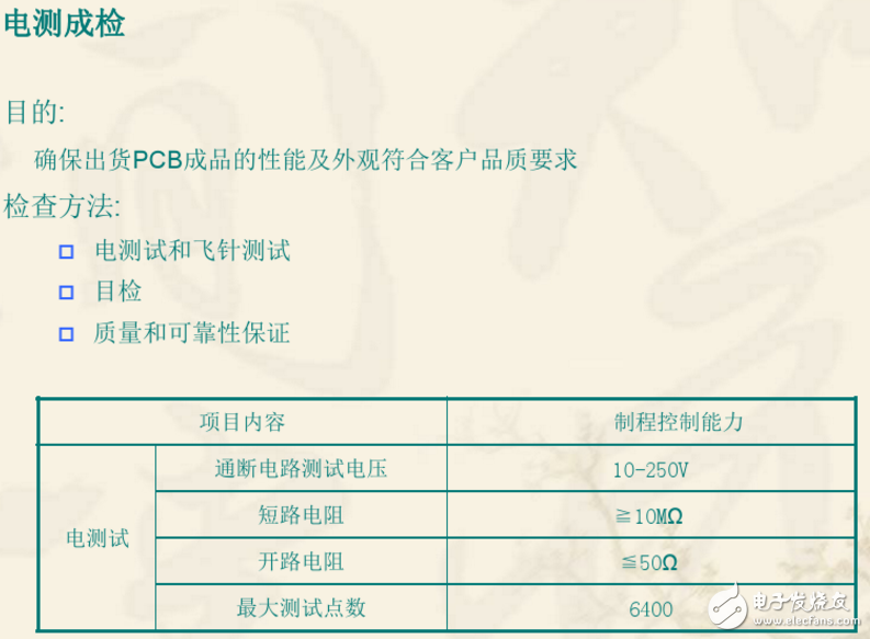
23. Test 100% circuit test of the PCB for customer-required performance to ensure that its functionality meets specifications.
24. The final inspection is for the board that has passed the test, and the appearance of the inspection is based on the customer's appearance inspection.
25. Packaging

Watch & Apple Airtag Screen Protector
TPU Watch Screen Protector, Transparent ​Watch Screen Protector, Watch Screen Protector Case, Apple Watch Case, Apple Watch Case Protector, Apple Watch Protective Case
Shenzhen Jianjiantong Technology Co., Ltd. , https://www.jonsun-sz.com