This article uses Altera's FPGA development tools to perform system verification before the ASIC stream on the SoC chip of the domestic Godson I processor IP core. The hardware code and software code generated by the collaborative design are run in full real-time mode to build an independent Operational, on-site monitoring verification platform.
1. Based on the Godson I processor IP core SoC chip
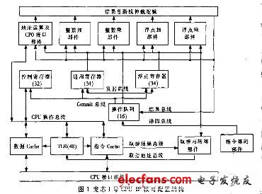
The Loongson I CPU IP core is a 32-bit processor core that combines the features of a general-purpose and embedded CPU. It uses a MIPS III-like instruction set with a 7-stage pipeline, 32-bit integer unit and 64-bit floating-point unit. It is highly flexible and configurable. Sexual, easy to integrate various standard interfaces. Figure 1 shows the configurable structure of the Loongson I CPU IP core. Users can choose and configure according to their own needs, thus customizing the processor structure that is most suitable for the user application.

Figure 1 Godson I CPU IP core configurable structure
The main configurable modules include: floating point components, multimedia components, memory management, Cache, coprocessor interfaces. The floating point component is fully compatible with the MIPS floating-point instruction set, and its associated system software is fully compliant with the ANSI/IEEE 754-1985 binary floating-point arithmetic standard. Floating point components mainly include floating point ALU components and floating point multiply/divide components, and users can choose whether to add according to their actual application. The media component multiplexes the Format field of the MIPS floating-point instruction and multiplexes the floating-point register file. The media instruction set basically corresponds to various operations of the Intel SSE media instruction set. Figure 2 shows the SoC system architecture based on the Godson I CPU IP core.

Figure 2 SoC system structure
The SoC chip supports the general MIPS32 instruction set with a frequency of up to 266 MHz. The built-in MAC network provides the MII interface. The memory interface supports both the SDRAM interface, the NOR Flash/ROM and the \AND Flash interface, and the special HPI interface can be directly Connected to the Y0IP CODEC chip; provides a wealth of other peripheral interface support, including PC interface, UART serial port, SP! Interface devices such as interfaces and AC97. Offering a rich GP10 interface, it provides an efficient single-chip solution for "network + voice" and industrial control applications.
2 FPGA verification platform design
2.1 FPGA development process
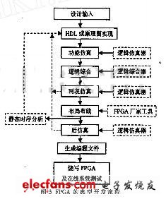
The typical development process of FPGA is shown in Figure 3. In Figure 3, the logic simulator mainly includes Modelsim, Verilog_XL, etc. The logic synthesizer mainly includes LeonardoSpectrum, Synplify Pro, FPGA Ex~press/FPGA CompilerII, etc. The FPGA manufacturer tools include Altera's Max+Plusll, Quartusll, and Xilinx's FoundaTIon ISE. , Alliance, etc. The design input is mainly in the form of schematic input and HDL input. Most designers, FPGA and ASIC engineers use the HDL platform. The design simulation mainly includes functional simulation and netlist simulation. The juice simulation requires RTL code or integrated HDL netlist and verification program. Sometimes the test data is needed. The test data may be the compiled binary file or use special tools. Data collected. The place and route tool utilizes the integrated generated netlist, the netlist of the calling module, translates the design into the original target process according to the layout and routing target, and finally obtains the data files needed to generate the programming bitstream. The input and output relationship that is generally required for place and route is shown in Figure 4. The layout and routing targets include the specific model of the FPGA used. The constraints include the pin position, the pin level logic (LVTIL, LCMOS, etc.) required clock frequency, sometimes including the layout of some modules, the location of the block RAM, and so on. In the general design, only the pin position and the required clock frequency are required. The correspondence between the logic port and the FPGA pin depends on the design of the PCB.

Resolver is a kind of commonly used angle detection component, because of its simple structure, reliable operation, and its accuracy can meet the general detection requirements

Resolver,Encoder Troubleshooting Resolver,Custom Resolver,Online Resolver
Yuheng Optics Co., Ltd.(Changchun) , https://www.yhenoptics.com