introduction
This article refers to the address: http://
At present, digital camera technology has made rapid progress, and it is constantly developing towards high resolution, high ISO, multi-function, ultra-thin, ultra-small, waterproof and shockproof. However, the quality of the photo image taken by the digital camera is the most important. The image quality of the image is related to the lens, CCD, DSP, etc., especially the hardware design of the image processing part is particularly important.
The image processing part hardware mentioned in this article contains the following parts. (see picture 1)
Selection of key components
(1) CCD photocoupler
There are many general types of CCD. According to the color of the filter, there are primary color CCD and complementary color CCD. The primary color CCD filter is sorted by green blue and red and green. The complementary color CCD filter is sorted by magenta green and green yellow. Basically, the primary color CCD has good color reproduction but poor sensitivity. The complementary color CCD has poor color reproduction but good sensitivity. Generally, digital cameras use more primary color CCDs. According to the charge transfer method, there are a full frame transfer design (FT) CCD, an interline transfer design (IT) CCD, and a frame line transfer design (FIT) CCD. The FT CCD device has a large area and a low price; the IT CCD has the smallest area and the lowest price; the FIT CCD has the largest area and the highest price, and the general consideration is that the general household digital camera uses the IT CCD.
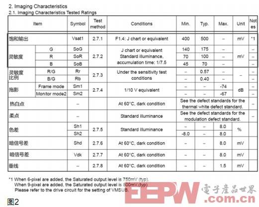
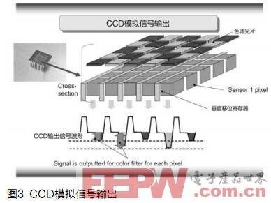
First, according to the design requirements of the camera, determine how many pixels are used by the CCD, and then confirm the appropriate size according to the collocation with the lens, and carefully understand the specifications of the CCD, and focus on confirming the value of the saturated output and sensitivity (Figure 2). A product with a large value. Simply put, a CCD is a device that converts an optical signal into an electrical signal (see Figure 3).
(2) IC AFE
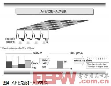
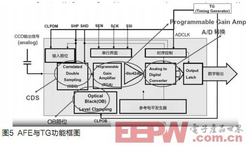
AFE analog front end, TG timing generator, CDS associated double sampler, usually integrated with CCD driver, ADC, etc., to form a whole CCD charge readout, sampling, amplification, analog to digital conversion processing unit IC AFE. Basically, as long as the CCD is selected, the processing unit AFE is also determined. The AFE is a device that converts the simulated electrical signal output by the CCD into a digital signal (see Figures 4 and 5).
(3) DSP digital processor
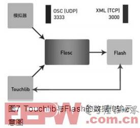
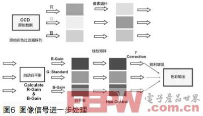
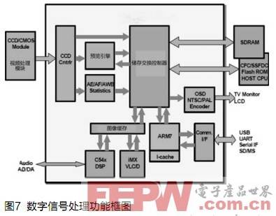
DSP mainly performs a series of processing on digital image signals obtained by AFE, such as white balance, brightness adjustment, color adjustment, γ correction, sharpening, white point, hot dry point correction, noise processing, compression, etc., generally according to the product. Design specifications, DSP manufacturers demonstrate actual effect evaluation, cost analysis and other decisions. (See Figure 6, Figure 7)
Circuit design
After the above key components are determined, the circuit design can be carried out according to the specifications provided by the manufacturer. This article uses Panasonic MN34542PAJ (12M pixels) for CCD, Panasonic NN12083A for AFE, and Novatek NT96433BG for DSP.
Circuit analysis
(1) The CCD uses two sets of -6V and +12V power supplies, of which +12V is simultaneously supplied to the CCD output current amplifying IC U3. The signal quality of the CCD output directly affects the image quality. Therefore, the noise of the +12V power supply is very high and needs to be smaller. 60mV (the smaller the better).
(2) In the AFE circuit, a simple RC filter composed of R210 and C242 is designed before the CCD signal enters the AFE, and the high frequency noise is filtered out. The power supply used in each part of the AFE has higher noise requirements, so three LDOs are used to purify the power supply, and +1.8V provides both TG and analog parts, separated by L200. H1/H2/HL/RG is used for driving transfer and clearing of CCD charge. The frequency is 40.5MHz, and the instantaneous current is large (60~80mA), which has a great influence on EMI. Increase the FL200/FL201 LC filter. improve.
PCB design
Considering the assembly requirements, usually a CCD part of the circuit uses a separate FPC, AFE/DSP and other circuits are placed on another PCB, through the FPC output connection.
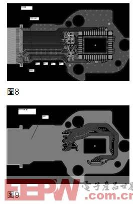
(1) CCD FPC design focus: First, the CCD output must be completely wrapped on both sides and the bottom, and the line width requires 8 mils (1 mils = 0.0254 mm) or more. The second is H1/H2/HL/RG priority routing, the two sides and the bottom should be completely packaged, the line width requires more than 6mils, and try to stay away from the CCD output signal (32mils or more) (see Figure 8, Figure 9).
(2) AFE/DSP part, CCD output, H1/H2/HL/RG requirements are the same as (1), and also need to pay attention to: First, C237/238/239/241/243/244/246 is used to provide reference level. It must be as close as possible to the CCD output DC blocking capacitor C240; secondly, at least one 0.1mF side capacitor should be placed next to each AFE power supply; third, the 40.5MHz crystal oscillator must be away from the CCD output signal.
debugging
After the sample is assembled, it must go through a complicated and cumbersome debugging process. There are many debugging projects, contents and steps. Only the adjustment of the sampling point of the CCD output (input) signal is introduced here, because this is very important for the quality of the image.
(1) Adjust H1/RG so that the CCD output P and D are approximately the same width (Figure 10).

(2) Adjust the SHP so that its rising edge is at the relative smoothness of the P segment of the CCD output signal. This is the reference point for the CCD output signal sampling comparison (black level) (see Figures 11 and 12).
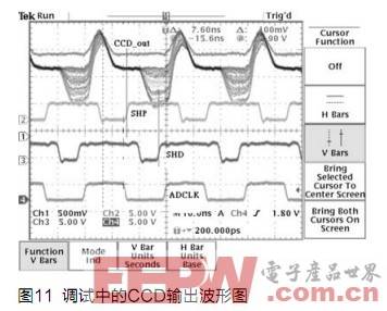
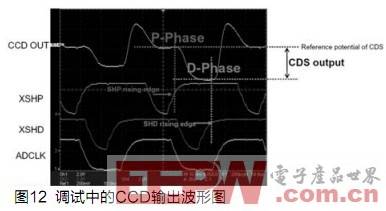
(3) Adjust the SHD so that its rising edge is at the maximum and relatively smooth amplitude of the D segment of the CCD output signal, which is the reference point for the CCD output signal luminance sampling.
Analysis and processing of common image defects
(1) There is a fixed bright bar on the left side of the picture.
Cause: The RG/HL drive current is too large.
Countermeasure: Adjust the RG/HL drive current to the appropriate (no overshoot)
(2) There is a fixed bright bar above the picture.
Cause: The RGVDD/HVDD current response is not fast enough.
Action: Increase the 0.01mF LOW ESR MLCC capacitor near the AFE IC RGVDD/HVDD PIN.
(3) There are some fixed vertical stripes in the picture.
Cause: The AFE TG timing does not match the CCD vertical drive requirement timing.
Countermeasure: Adjust the AFE TG timing to match the CCD vertical drive requirement timing.
(4) There are some fixed horizontal stripes in the picture.
Cause: The exposure time of different frames is different.
Countermeasure: Adjust the relevant settings of the DSP to make the exposure time consistent.
(5) There are unfixed diagonal stripes in the picture.
Cause: The AFE CDS/CCD/TG power supply is noisy.
Countermeasure: Adjust the AFE CDS/CCD/TG power supply design to minimize power supply noise.
Conclusion
In this paper, the hardware design of the digital camera image part gives a specific implementation plan from the selection of components to the fabrication of the circuit, the wiring of the PCB, etc., and some key considerations often encountered in design and debugging. in-depth analysis.
Shenzhen Innovative Cloud Computer Co., Ltd. , https://www.xcypc.com