According to Shanghai Jinma analysis: the elisa kit combines the specific reaction of antigen and steroids with the high-efficiency catalysis of enzymes on substrates. Since the reaction of the antigen and the antibody is carried out in the well of a solid phase carrier, a polystyrene microtiter plate, after each reagent is added, the excess free reactant can be removed by washing to ensure the specificity of the test result. And stability. In practical applications, there are many specific method steps through different designs. Namely: an indirect method for detecting antibodies (panel a), a double antibody sandwich method for detecting antigens (panel b), an antigen competition method for detecting small molecule antigens or haptens, and the like.
According to the research experience of Shanghai Jinma Biological for many years, our company recommends the ELISA kit double antibody sandwich method and ELISA indirect method. The following six points are the test method steps, welcome to read and read.
1. Coat: The antibody was diluted to a protein content of 1 to 10 μg/ml with 0.05 M PH9. 牰 carbonate coating buffer. 0.1 ml was added to the reaction well of each polystyrene plate at 4 ° C overnight. The next day, the solution in the well was discarded and washed 3 times with washing buffer for 3 minutes each time. (referred to as washing, the same below).
2. Loading: Add 0.1 ml of the sample to be tested diluted in the above-mentioned coated reaction wells, and incubate at 37 ° C for 1 hour. Then wash. (Do blank holes, negative control wells and positive control wells at the same time).
3. Add enzyme-labeled antibody: Add 0.1 ml of freshly diluted enzyme-labeled antibody (diluted titration) to each well. Incubate at 37 ° C for 0.5 to 1 hour and wash.
4. Add substrate liquid to develop color: Add 0.1 ml of temporarily prepared TMB substrate solution to each reaction well at 37 ° C for 10 to 30 minutes.
5. Stop the reaction: Add 0.05 ml of 2M sulfuric acid to each reaction well.
6. Judgment of results: The results can be observed directly on the white background with the naked eye: the darker the color in the reaction well, the stronger the positive degree, the negative reaction is colorless or very light, according to the depth of the color, with "+", The "-" sign indicates. O·D value can also be measured: on the ELISA kit detector, at 450 nm (if ABTS color development, 410 nm), the blank control well is adjusted to zero and then the O·D value of each hole is measured, if it is greater than the specified negative It was positive by 2.1 times the control OD value.
We will provide our customers with high quality products and experimental technology solutions with a high degree of responsibility and excellent product quality. Rich experience, excellent quality, sufficient inventory, accurate delivery time, and competitive price all guarantee the most professional and best service we provide to you. Promotions, all ELISA kits are available at very low discount prices, free technical guidance, free testing services, welcome new and old customers to inquire details. 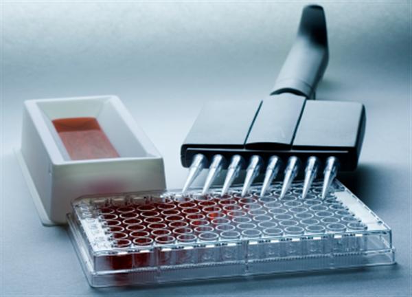
Innosilicon Asic Miner:Innosilicon A9 ZMaster,Innosilicon A9++ ZMaster,Innosilicon A9+ ZMaster
Innosilicon is a worldwide one-stop provider of high-speed mixed signal IPs and ASIC customization with leading market shares in Asian-Pacific market for 10 consecutive years. Its IP has enabled billions of SoC's to enter mass production, covering nodes from 180nm to 5nm across the world`s foundries including: GlobalFoundries, TSMC, Samsung, SMIC, UMC and others. Backed by its 14 years of technical expertise in developing cutting-edge IPs and ASIC products, Innosilicon has assisted our valued partners including AMD, Microchip and Microsoft to name but a few, in realizing their product goals.
Innosilicon team is fully devoted to providing the world's most advanced IP and ASIC technologies, and has achieved stellar results. In 2018, Innosilicon was the first in the world to reach mass production of the performance-leading GDDR6 interface in our cryptographic GPU product. In 2019, Innosilicon announced the availability of the HDMI v2.1 IP supporting 4K/8K displays as well as our 32Gbps SerDes PHY. In 2020, we launched the INNOLINK Chiplet which allows massive amounts of low-latency data to pass seamlessly between smaller chips as if they were all on the same bus. With a wide range of performance leading IP in multiple FinFET processes and 22nm planar processes all entering mass production, Innosilicon's remarkable innovation capabilities have been proven in fields such as: high-performance computing, high-bandwidth memory, encrypted computing, AI cloud computing, and low-power IoT.
innosilicon zec miner,Innosilicon A9 ZMaster,innosilicon a9 50ksol miner,innosilicon a9 miner,a9 50ksol zmaster
Shenzhen YLHM Technology Co., Ltd. , https://www.sggminer.com